PCB Design
To ensure high power efficiency, the most important consideration in the PCB design is properly layout of the system and routing with adequate width to reduce efficiency drop due to parasitic resistance. Given that the range of the resistance of common audio speaker is usually within few $\Omega$, any resistance in the power lines will appear in series with the internal parasitic resistance introduced by transistor thus significantly lower power efficiency rendering less power delivered to the load.
A 9V battery is used for the power supply of the chip. Two 1.8V LDO generated the power VDD and analog VDD seperately. A 0.9V reference voltage was generated from the analog VDD by voltage divider circuit.
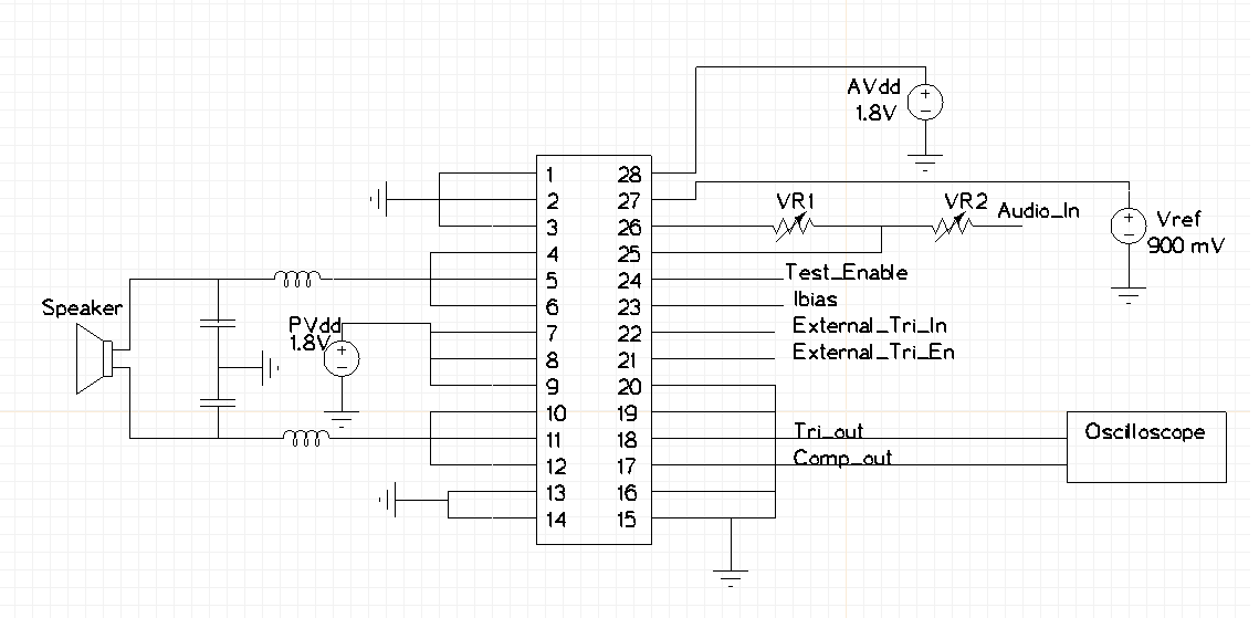
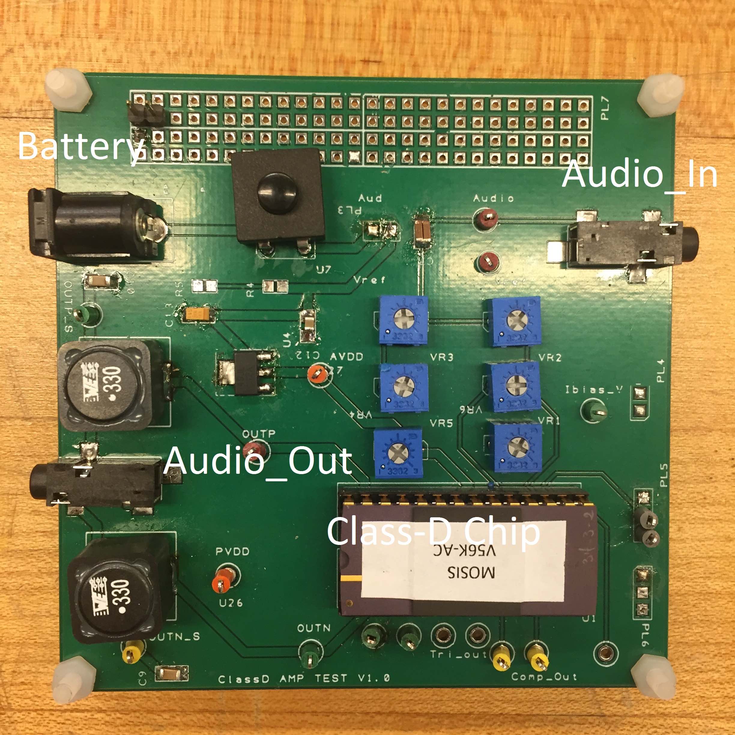
Figure 1 shows the block diagram of all the components on the PCB while Figure 2 shows the photo of the actual PCB annotated to show the most important parts. The PCB layout and schematic are drew by PCB Artist.