Block Diagram
Pulse Width Modulation Block
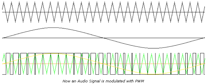
In our design, the PWM signal is generated by comparing the audio input with high frequency triangular wave. The output of the comparison is a pulse train at the frequency of the triangular wave since the frequency of the triangular wave is much higher than the frequency of the audio input. Figure 1 shows the typical operation.
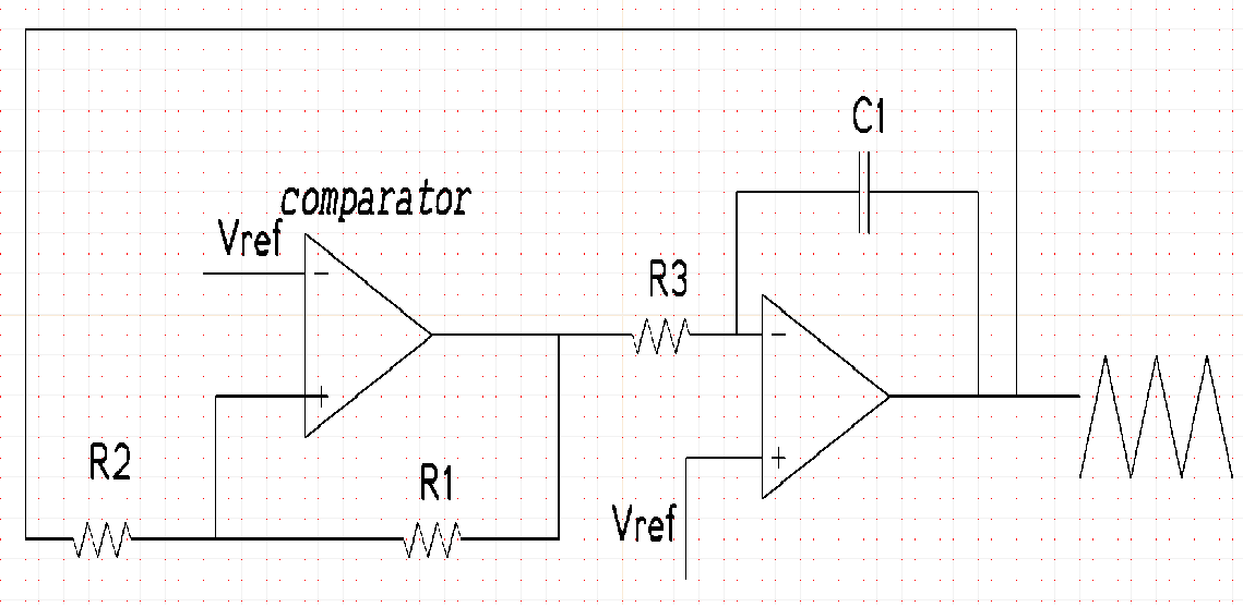
Triangular Wave Generator
An internal triangular wave generator was implemented in the class-D amplifier. It is implemented by an integrator and a Smith trigger in Figure 2. The peak to peak amplitude of the triangular wave is given by $\dfrac{R_2VDD}{R_1}$, and the period is given by $\dfrac{4R_3CR_2}{R_1}$. In our design, we choose $R_1 = 24k$, and $R_2 = 16k$, $R_3 = 100k$, $C_1 = 5pF$. So the triangular wave should have 750KHz frequency and 1.2V peak to peak amplitude.
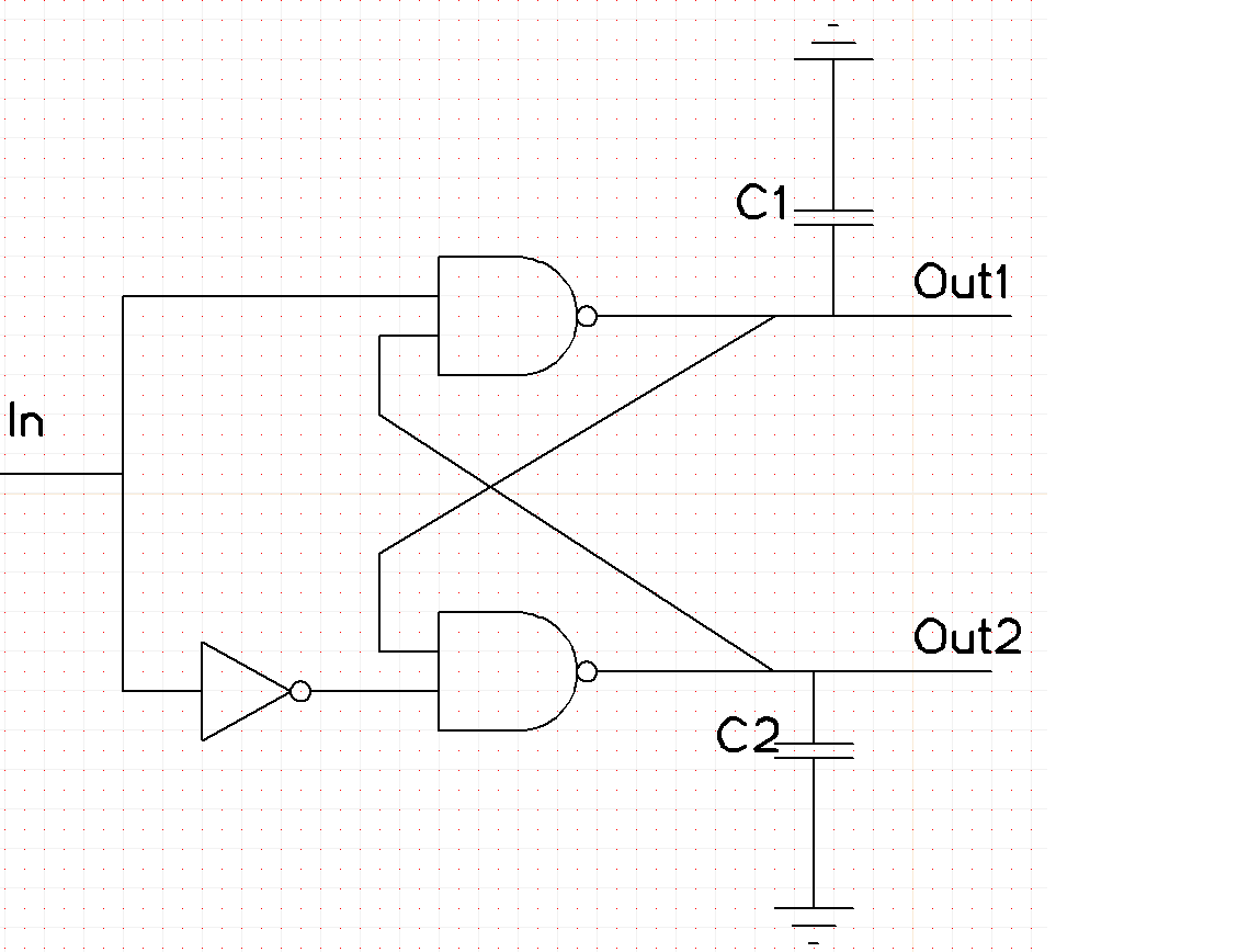
Non-Overlap Generator
The output driver stage of class-D amplifier consists of a switch connects to VDD, and another switch connects to VSS. The dead time is defined as the time interval that neither of two switches are on. For ideal switch, the dead time can be made arbitrarily small. However, due to the delay and the finite slope of the control signal, we have to introduce some dead time intentionally so that there isn't any time both of the two switches are on. When both of the two switches are on, a short path is created from VDD to VSS, which not only affects the power efficiency, but may also damage the chip.
The schematic of non-overlap generator is shown in Figure 3. This is a standard Set-Reset circuit, and the dead time is determined by the capacitor value C. 20ns dead time was chosen for our design.
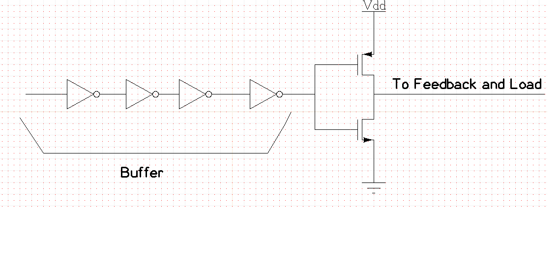
Buffer and Output Stage Driver
The output driver are used to provide large current to the load, shown in Figure 5. The finite on resistance of the output driver is the major cause of the efficiency lost. The efficiency is approximated by
\[ \eta = \dfrac{R_L}{R_{op}+R_{on}+R_L} \]We designed the size of the output stage to have an efficiency about 90%.
Buffers are needed to drive the large output stage MOS. Buffers are inverters in our design.
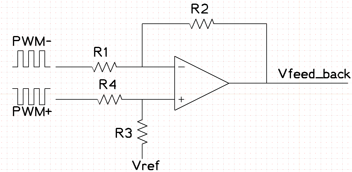
Feedback Adder
The main purpose of the feedback network is to feedback the error signals to the input to reduce the distortion. In our design, since the input is single ended, and the output is differential, a differential to single conversion needs to be achieved, and the error information needs to be added. The task can be completed by using an opamp as adder to add the error information from the differential signal. The circuit is shown in Figure 5. Then the signal $V_{feed\_back}$ will be connected to a classic resistor feedback network to the input of the system, where the gain can be adjusted by changing the ratio of the two resistors.
\[ V_{feed\_back} = PWM^+\dfrac{R_3}{R_3+R_4}\dfrac{R_2+R_1}{R_1}-PWM^-\dfrac{R_2}{R_1} \]