
Test Result
After we received the chip from MOSIS, we started to test our design. First we verified the pin diagram of the DIP28 package. Second we tested our chip on the breadboard to verify the functionality of each building blocks (including two OTAs and one comparator). Third, we tested our whole system on breadboard to verify the functionality. Fourth, After we received our PCB from MOSIS, we tested our PCB without the chip to make sure the DC supply voltage of each point is just as our design. We tested our chip with our chip, Arduino and display to verify the functionality of our system. At last we tested the frequency response of the system with signal generator.
BREADBOARD TEST
1. DC operating point test
To make sure the DC operating points of OTAs were right, we put the OTA in unity feedback to see if the negative input can track the DC operating points of the positive input. First the power supply was set to 1.8V, common mode voltage Vcm was set to 0.9V, Vss was set to ground and the 50 uA current source was provided with a 50KΩ potentiometer, then the Vcm was fed into the OTA positive input vi+. Measured the DC voltage level at the positive input and compared it with the Vcm. Measurement results showed that the DC voltage at the OTA negative input was 0.9V. Then the OTA has a certain gain to stabilize the DC operating point.
2. Functionality test
First of all, we would like to know if the OTAs and comparator on chip works as we expected. We first implement our system on a breadboard. The OTA's functionality test result is shown blow.
Functional Test of OTA
The comparator's functionality test result is shown blow. Vref is set as 1.25V and it has a threshold voltage of 105mV as expected.
Functional Test of Comparator
For overall system test, the PPG sensor was used to generate the sinal needed. Set Vdd to 1.8V, Vcm to 0.9V, Vss to ground, and provided 50uA current source with 50KΩ potentiometers at Iref. Applied the signal at the input of the 2nd order high pass filter, tested the output of each important node in the system. We found an important defect, which is the settling time is too long. This implies that the 10nF capacitors in the low pass filters are so large that the slew rate of the two OTA stages are not high enough to handle large sudden change in the input signal. For example, when you plug your finger or remove your finger from the sensor, the OTAs may take several seconds to charge up these capacitors and then the system can work normally, which is certainly not what we want.
So we change the capacitors from 10nF to 1nF to increase the slew rate of the 2 OTA stages, and still make our system immune to noise frequency higher than 40 Hz.
PCB Test
1. Functionality test
First, we test each DC node voltage on the PCB before we plugged in the sensor and our PPG chip.
Then, we tested each waveform at the important nodes in the system. Following the signal path, all the waveforms are listed below.
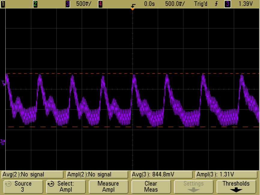
Input Signal From Sensor
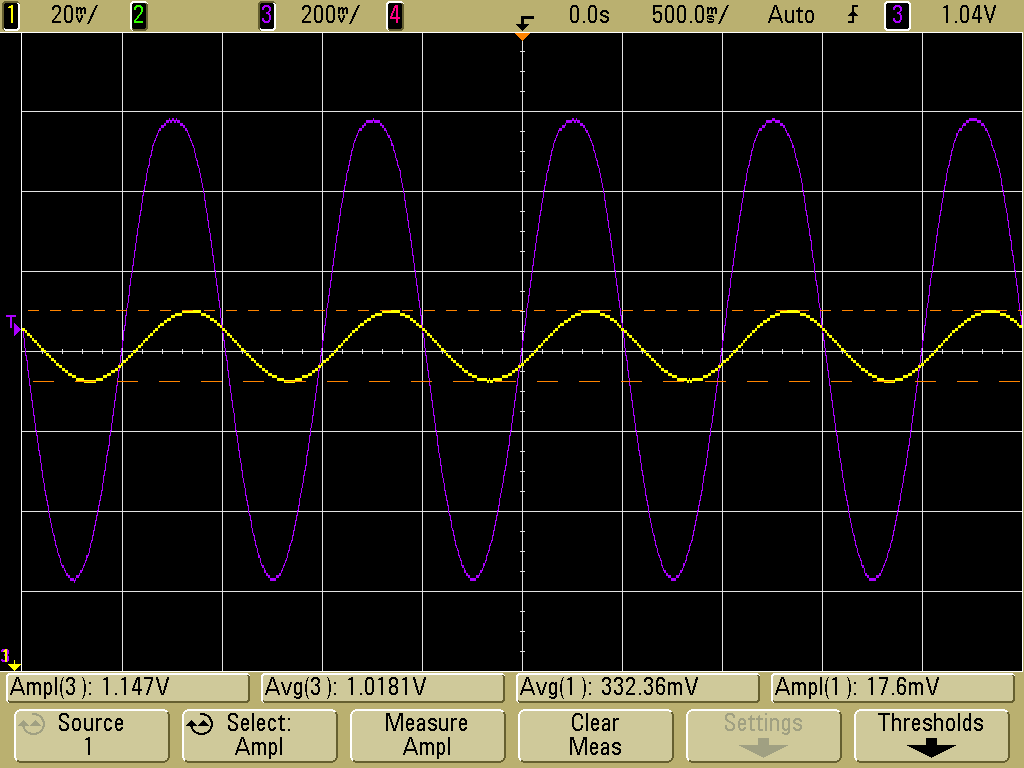
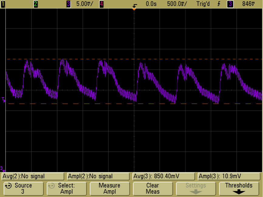
Output Signal of First Stage OTA
Comparing the signal between sensor and OTA1 output, we can see the average value of the output voltage from the first OTA stage becomes more stable, which means the effect from respiration has been reduced a lot by the 2nd order high pass filter.
Also,the amplitude of heartbeat signal has been increased by 130 times. Av1=1310/10≈130V/V
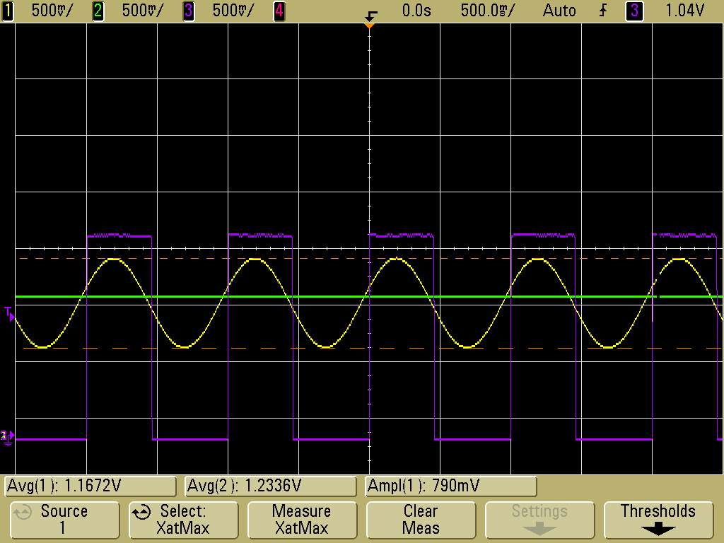
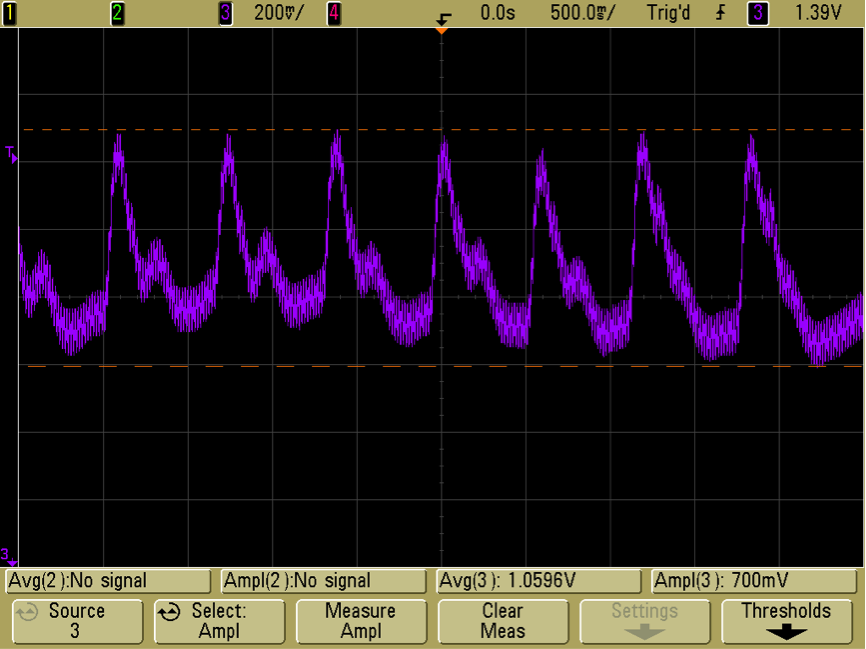
After the first stage OTA, the signal goes into a potential meter and then feed into the second high pass filter.
Input Signal of Second High Pass Filter
After the potentiometer, which is used to reduce the amplitude of the signal to make it not saturate the following OTA stage, the signal is reduced to 11mV.
Av2=11/1.31=8.4mV/V
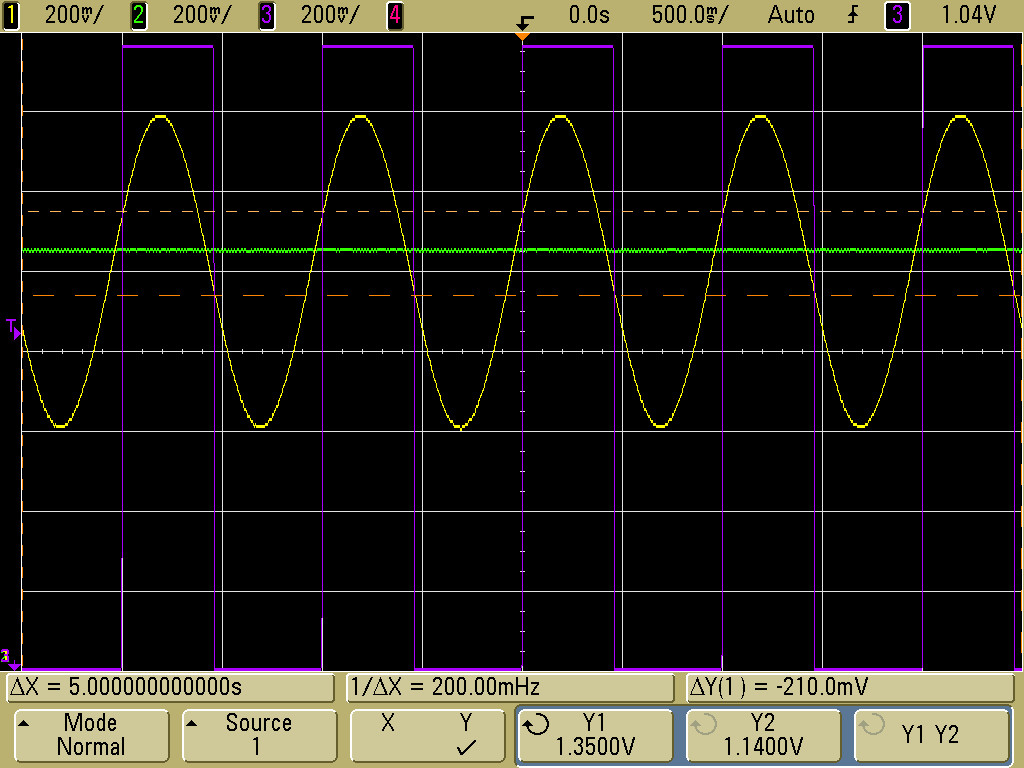
Then the signal feed into a low path filter and feed into the second stage OTA.
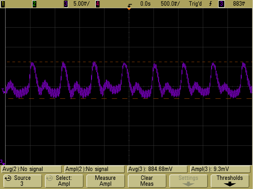
Input Signal of Second Stage OTA
Output Signal of Second Stage OTA
After the second OTA stage, the amplitude of heartbeat signal has been increased by 75 times.
Av3=700/9.3≈75V/V2. Frequency Response test
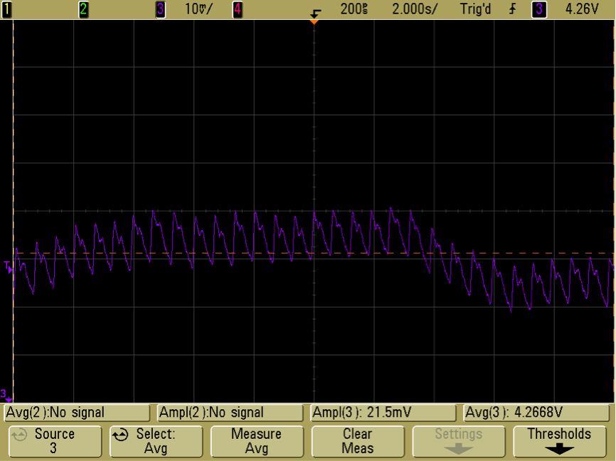
We used the signal generator to generate a frequency tunable sine wave input signal with 2mVp-p, and connected to the signal input of the whole system. We changed the input signal frequency from 0.5Hz to 100Hz, and tested the output of OTA2 at each different frequency.
We found that at 0.78Hz, we got the 3dB compression at low frequency from the overall high pass filter of the system.
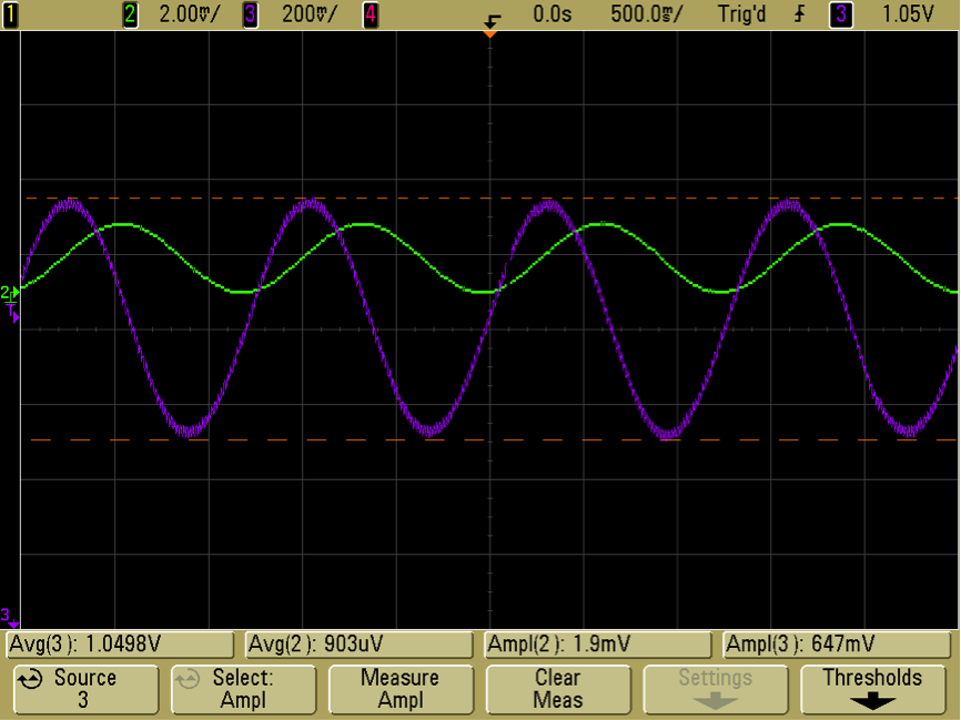
Input and Output Signal at 0.78 Hz
We also found that at 36 Hz, we got 3dB compression from the overall low pass filter of the system.
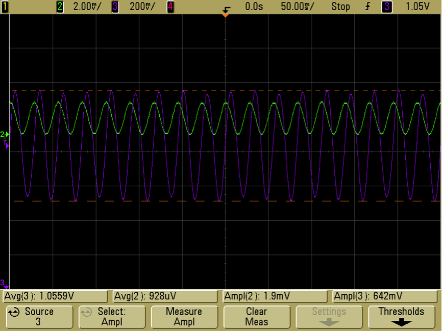
Input and Output Signal at 36 Hz
To get the frequency response of the system, we tested input and output of the system at multiple frequency, and get the following table.
| Frequency(Hz) | Vp-p of OTA2 output(mV) | Gain(dB) |
|---|---|---|
| 0.5 | 462 | 47.3 | 0.55 | 480 | 47.6 |
| 0.58 | 508 | 48.1 | 0.59 | 520 | 48.3 |
| 0.6 | 545 | 48.7 |
| 0.78 | 647 | 50.2 |
| 1 | 740 | 51.4 |
| 2 | 880 | 52.9 |
| 3 | 910 | 53.2 |
| 4 | 910 | 53.2 |
| 32 | 690 | 50.8 |
| 35 | 655 | 50.3 |
| 36 | 642 | 50.1 |
| 37 | 636 | 50.0 |
Note:
1. We increase the overall gain of the system by changing the potentiometer between two OTA stages to make the frequency response test more immune to disturbance from the environment and more accurate. But this change has little effect on the 3dB bandwidth of the system and only affect the amplitude of the gain.
2. The gain of our system is designed to be tunable.
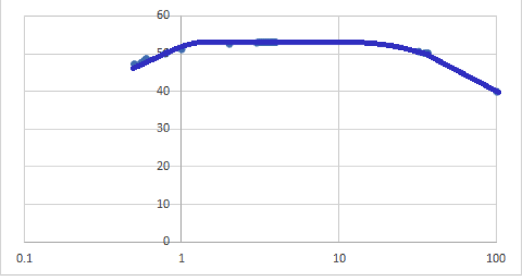
Frequency Response of the System
Conclusion
Our PPG system has a wider bandwidth than our former design, but has a faster settling time. There's a tradeoff between the speed and the bandwidth. We think that we may optimize our system by changing the capacitors in two low pass filters to a value between 1nF and 10nF, which can give us a reasonable speed of settling and a narrower bandwidth.