
Component Design
In our design, there are three main component on the chip, 2 OTAs and a comparator. Because the OTA are using the same way and the gain is set by feed back loop, so we can use the same OTA for both of them.
1. OTA Design
1.1 Structure
We choose the structure of two-stage Miller OTA for the following reasons:- Two stage OTA has higher gain.
- No stack of devices improve output swing.
- Miller Capacitor and resistor offers more freedom of adjust frequency response.
- Easier to design biasing circuit.

Schematic of OTA
1.2 Sizing
According to the gm/Id curve of a 180nm CMOS technology, the size of transistors in the OTA are shown as the following table.
| NAME | nfet1, nfet2 | pfet1-4 | ncs1-9 | C0 | RPC1 |
| SIZE | 20um/1um/4 | 40um/1um/8 | 12um/2um/2 | 20um/40um/4pF | 1um/8um/1.4kΩ |
1.3 Simulation Result
1) Open loop:

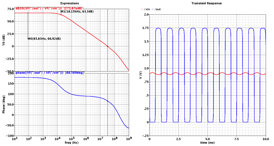
OTA Open Loop Simulation
Open loop Gain=66.92dB
3dB Bandwidth=18.15kHz
fT=40.3MHz
2) Loop Gain:

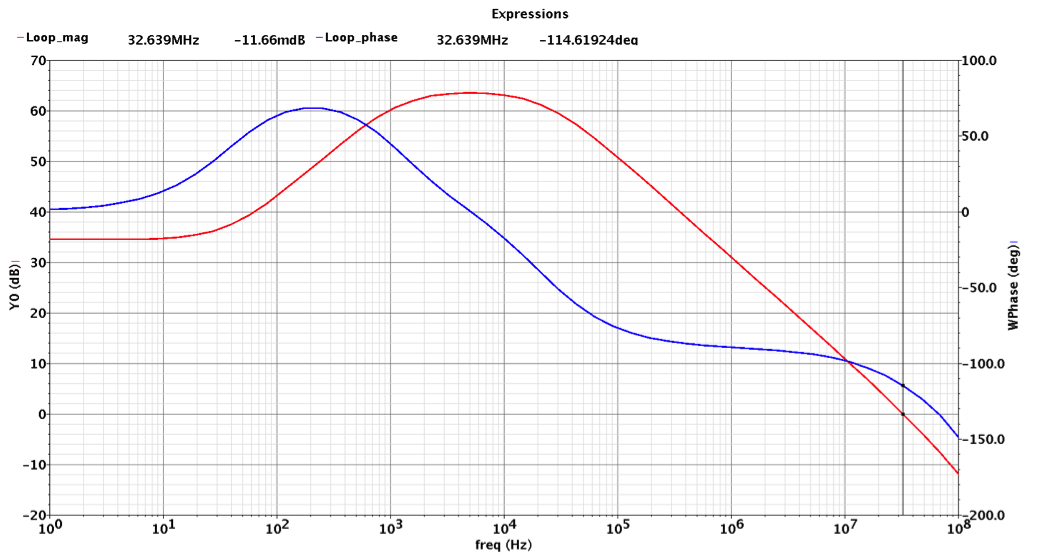
OTA Loop Gain Simulation
loop Gain=32dB
Phase Margin=66.3dB
3) Close Loop PVT:

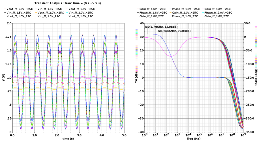
OTA Close Loop PVT Simulation
Gain=32dB
Bandwidth=40Hz
4) Step Response In Close Loop:
OTA Step Response Simulation
Slew Rate=386V/s
2. Comparator Design
2.1 Structure
Because of the noise in our system, we design the comparator with intrinsic hysteresis to make the comparator more immune to disturbance from the environment and noise in the system. We use a simple comparator with internal positive feedback as our hysteresis comparator structure[4]. The hysteresis of the comparator is 110mV.
Schematic of Comparator
2.2 Sizing
To have a hysteresis of 110mV, we sized our transistors as follows
| NAME | nfet1, nfet2 | nfet3,nfet4 | pfet1,2,5,6 | pfet3,pfet4 | ncs1-5 |
| SIZE | 20um/1um/4 | 1um/1um/1 | 5um/1um/1 | 20um/1um/4 | 12um/2um/2 |
2.3 Simulation Result
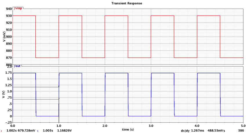
1) Transient Simulation:
The transient simulation result at typical corner is as follows. We apply a sine wave at the input and the reference voltage is set to be 0.9V.
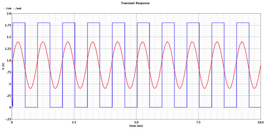
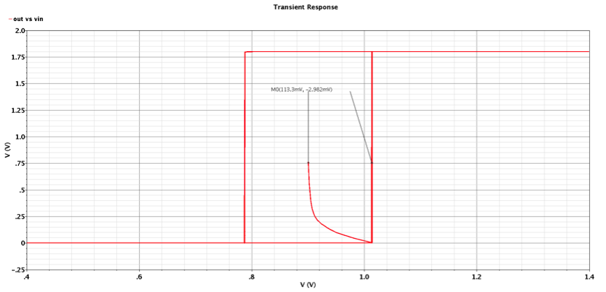
Comparator Transient Simulation
2) PVT Simulation:
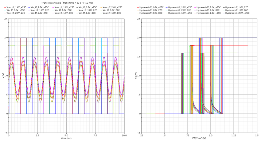
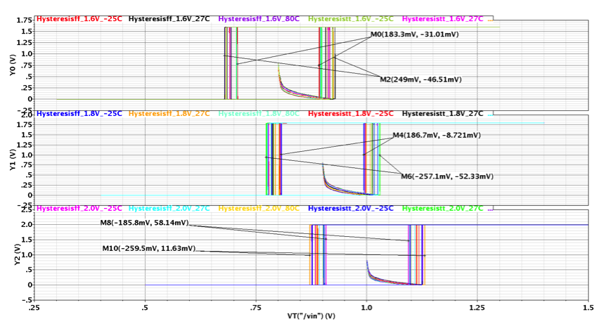
Comparator PVT Simulation