
IC Layout
The figure below shows the layout and die photo of JSQX6350. Three pins were used as VDD and another three for ground. The blocks were distributed along the die to minimize the trace resist. We use 18 pins in total.
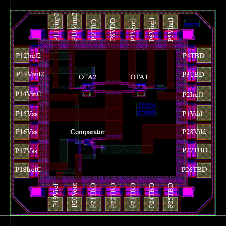
Layout of JSQX6350
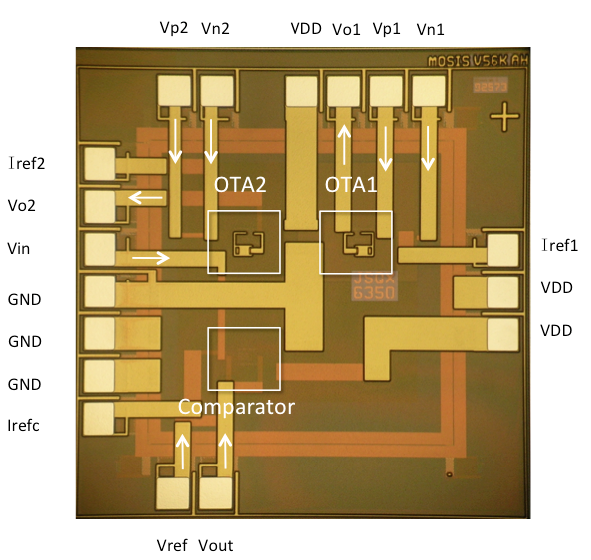
Die Photo of JSQX6350
OTA Layout
The figure below shows the layout of the OTA. In our design the gain of the amplifier is controlled by the feedback hence the two OTA are essentially the same. Inputs are coming from left side and output to the right.
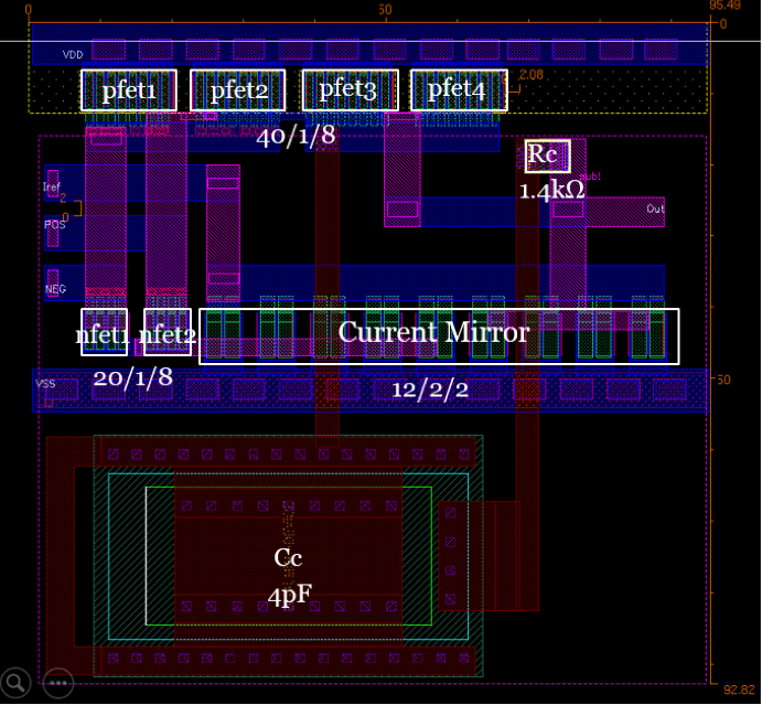
OTA Layout
Comparator Layout
The figure below shows the layout of the comparator. Inputs are coming from left side and output to the right.
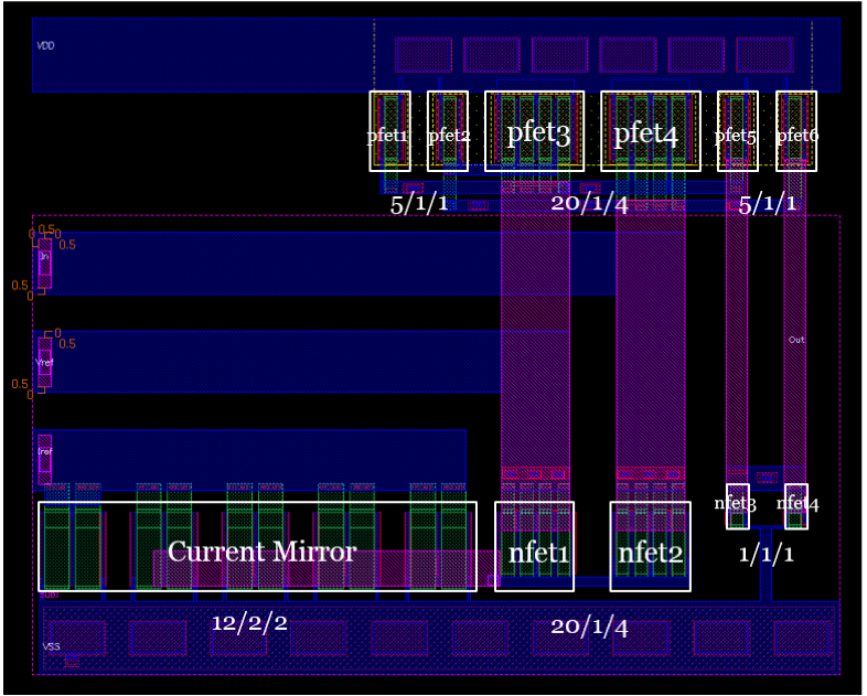
Comparator Layout