Testing
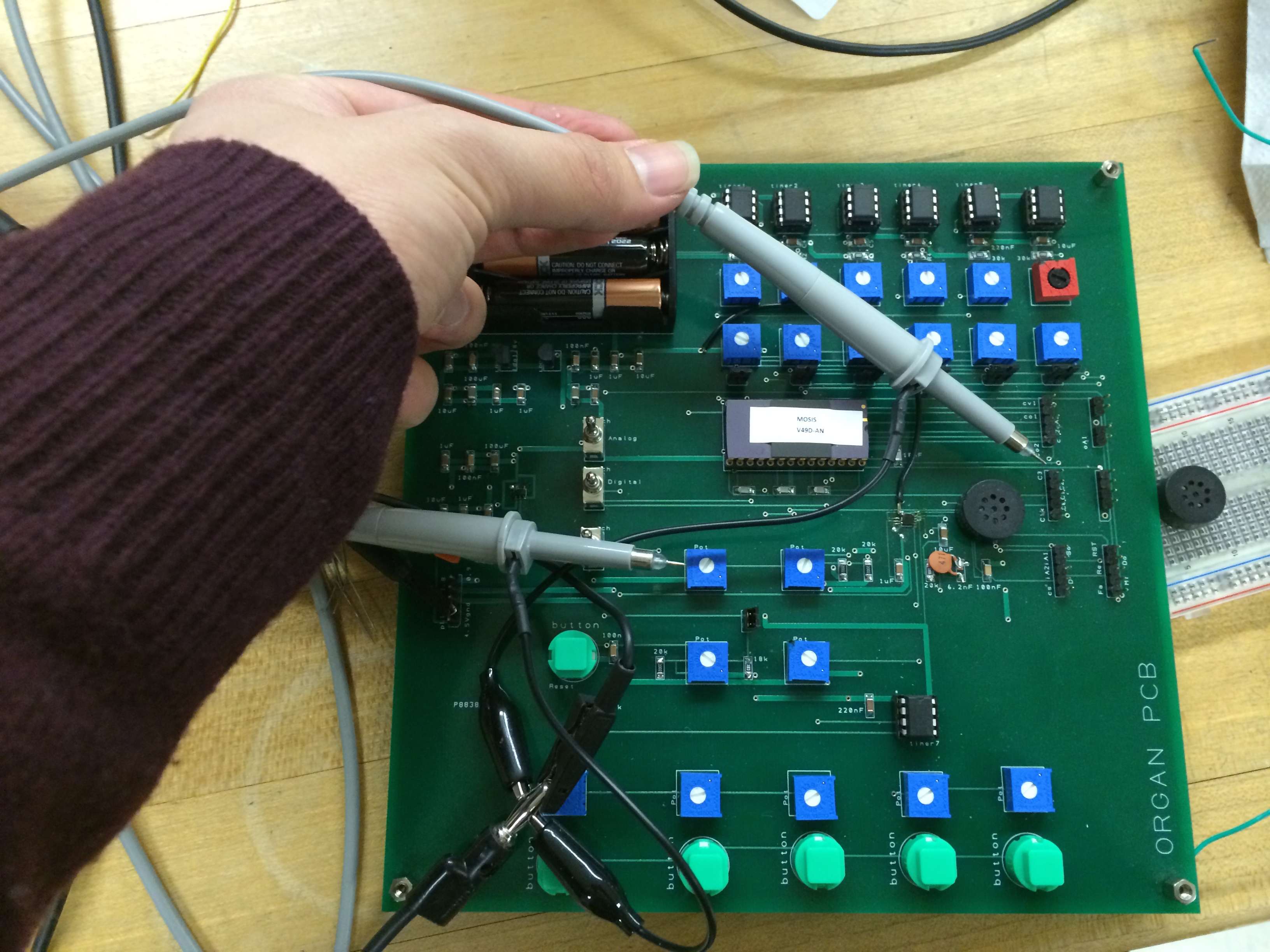
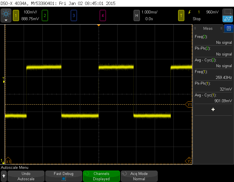
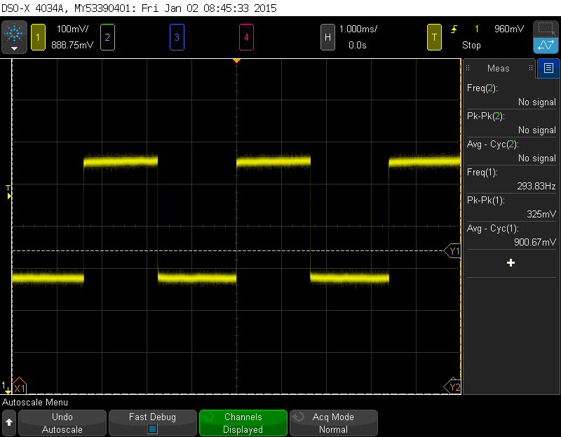
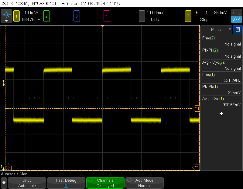
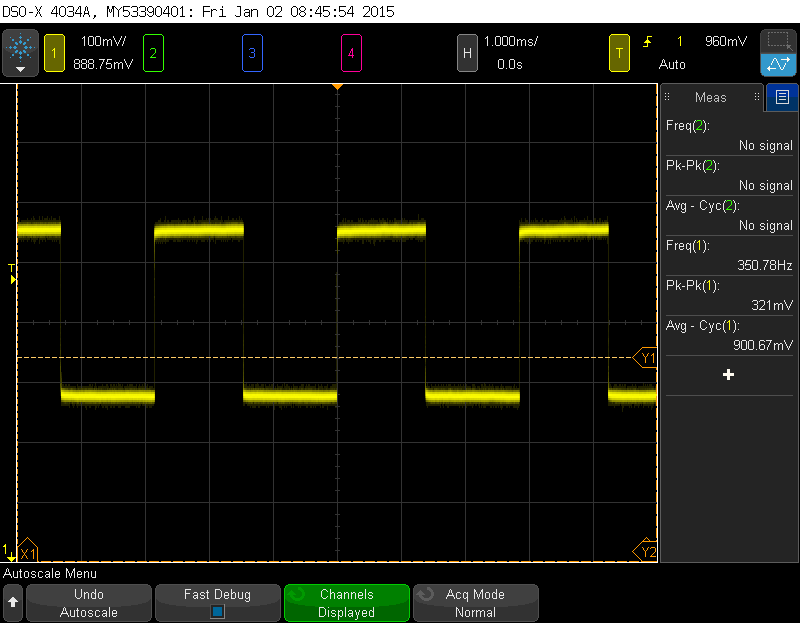
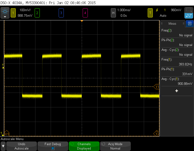
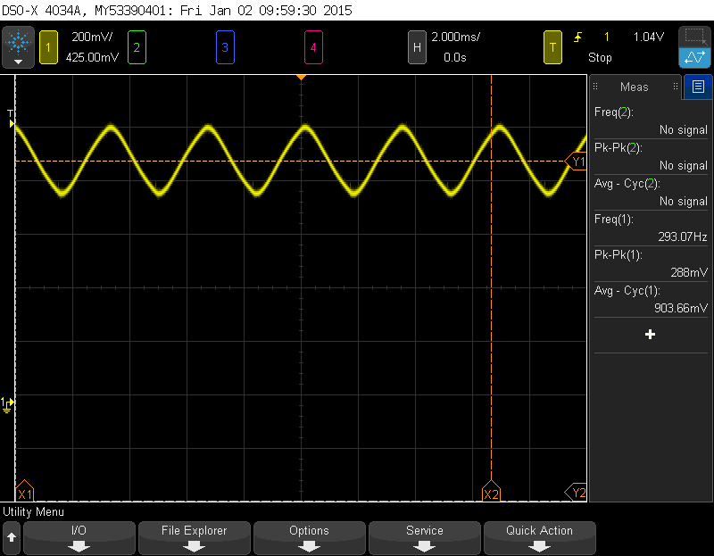
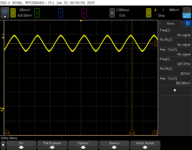
With the Electronic Organ chip and the Printed Circuit Board (PCB) in hand, the testing procedures started. The PCB was first checked. As shown in Figure 1, before the IC was plugged into the socket on the board, signals at each input bin were verified, including note frequencies, input ranges, clock signal, current source, reset and functionality of toggling switches. This procedure was executed by first putting three AAA batteries into the battery holder on the board, which supplies 4.5V. The 3V voltage regulator provides the power supply for 555 timers and the power amplifier. The 1.8V voltage regulator provides power supply for the Electronic Organ Chip. The 0.9V voltage regulator provides the virtual ground. Figure 2 shows the input signals of the IC from the output of 555 timers with tuned frequencies based on the international pitch standard (See Table 1 in Overview).
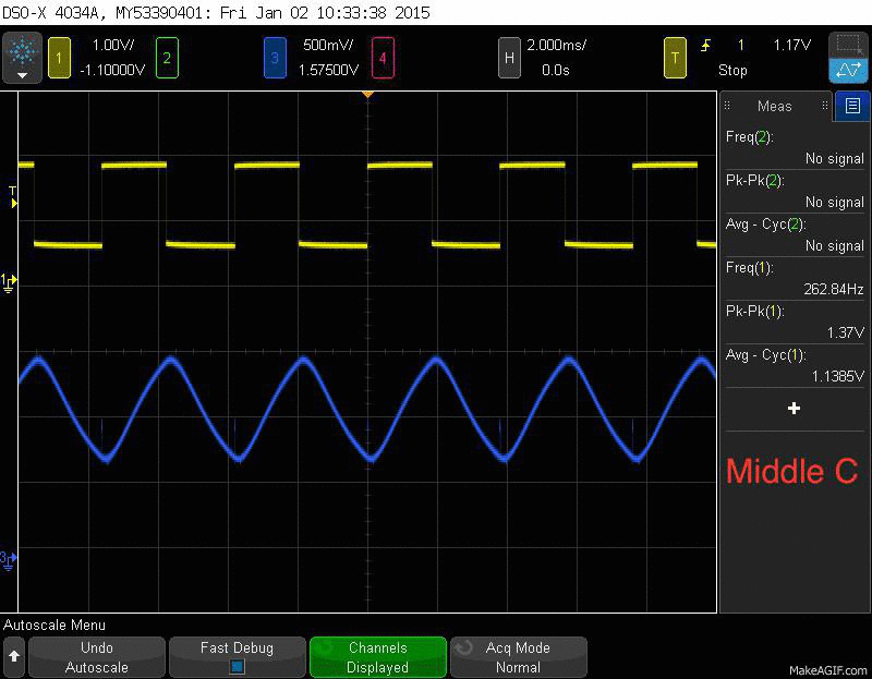
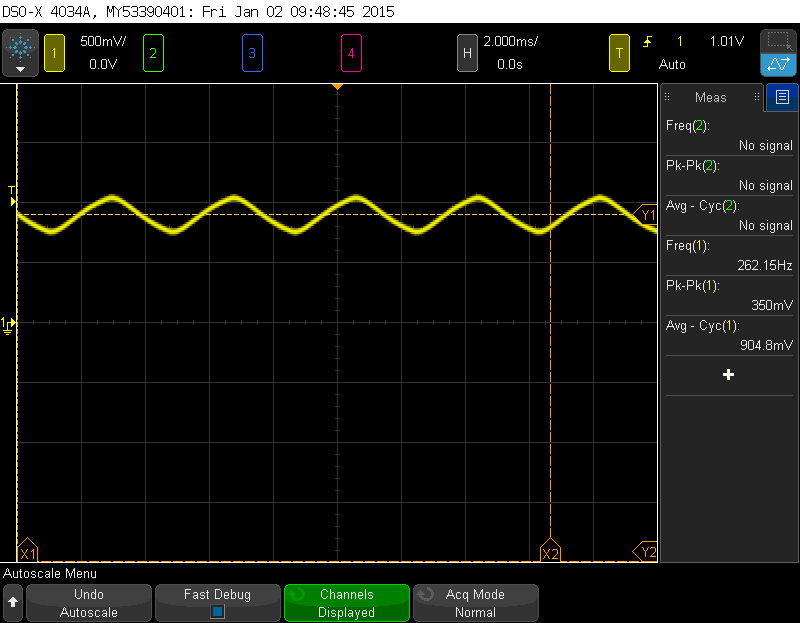
With the Printed Circuit Board worked, the chip was tested on a breadboard by applying a 1.8V power supply and a ground. DC biasing points for the op-amp design were first checked. Next, by giving a square wave shown above, the output of the low pass filter was measured and shown in figure 3, showing the low pass filter is functioning.


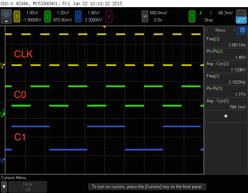
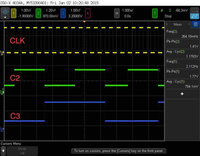
The crucial part of the digital design is the JK Flop based 4-bit Synchronous Up counter. In order to achieve auto play, the counter must increment with the negative edge of the clock input. Therefore, the counter's output was monitored and checked by feeding a 2 Hz clock to the input of the chip. The counter's outputs are C3, C2, C1 and C0. C0 increments with the negative edge of the clock. C1 increments with the negative edge of the clock when C0 is 1. C2 increments with the negative edge of the clock when both C0 and C1 are 1. C3 increments with the negative edge of the clock when C2, C1 and C0 are 1. When the counter reaches 15, it resets itself. Figure 4 and Figure 5 show the testing result.
In the next step, the chip was plugged onto the PCB. Both auto play mode and user play mode were tested by monitoring the input and the output of the IC. Figure 5 demonstrates the result for each note frequency. After this testing procedure, the power amplifier with a 8 ohm speaker is connected to the output and the chip. Both user play mode and auto play mode worked well. The maximum current drawn from the three AAA batteries with Auto Play Mode on was about 27mA and the maximum power consumption was about 120mW.