Implementations
Analog Circuit Design
The square wave to sine wave converter was designed based on Sallen-Key 2nd low-pass filter topology. Equation (1) shows the transfer function of this circuit and Equation (2) illustrates the cut-off frequency. The square wave input is buffered first in the IC and then low-pass filtered through this block. The cutoff frequency of the low-pass filter was designed to be 350Hz to eliminate higher order Fourier coefficients and noises.
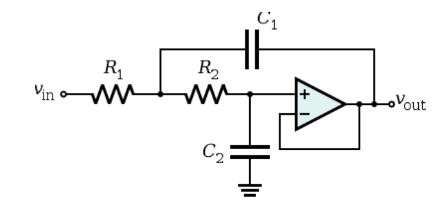
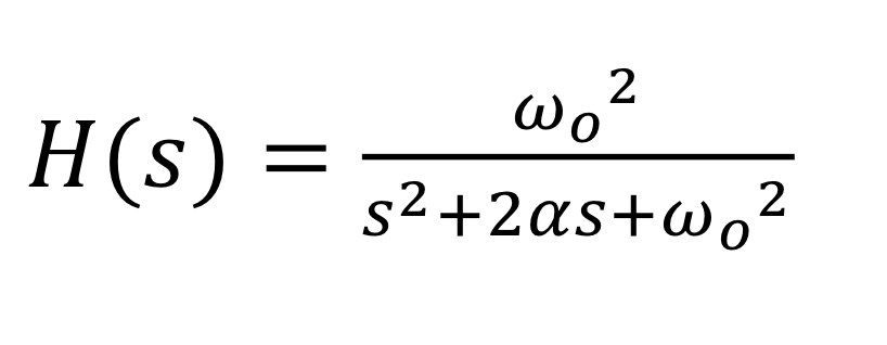
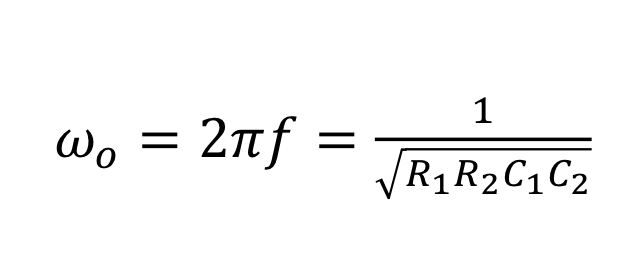
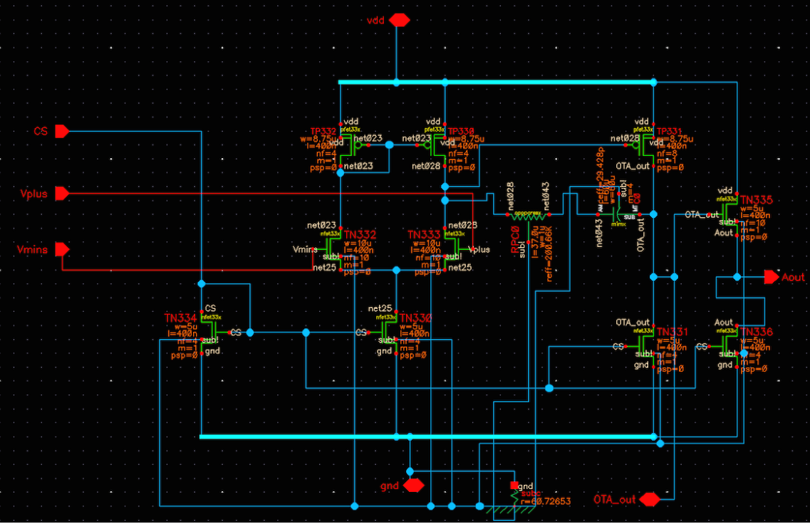
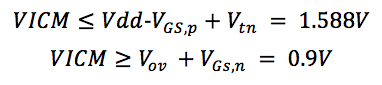
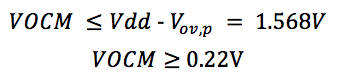
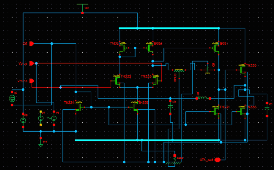
Figure 2 demonstrates the op-amp design for the low-pass filter.The design uses IBM 180um 1.8V transistors. The differential pair contains two nfets as the first stage. The second stage is a common source amplifier. There is another stage of source follower as the buffer to reduce the output impedance. Common-mode input and output ranges are shown in the following equations:
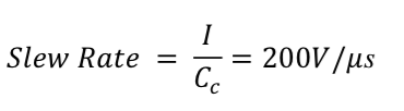
The common mode rejection ratio and slew rate is obtained by the following. The CMRR is about 30DB and the slew rate is 200V/us.

In the next section, the stability of this op-amp design is discussed.
A Miller capacitor and a compensating resistor were placed between the first
stage and the second stage to improve the stability of the op-amp. The Miller capacitor is about 1pF,
which gives a unity gain frequency of 7MHz. For the lead compensate resistor,
in order to make it beneficial for the phase margin, we must have it at least 1/gm,p = 567.
Therefore, a 1K resistor was placed here for the best phase margin.
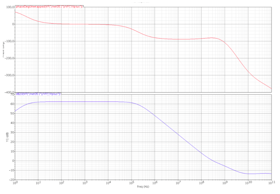
AC analysis was performed based on the configuration shown in figure 3, which is for the open loop gain.
An ideal low pass filter at cut-off frequency 0.1Hz was placed in the feedback loop for biasing the inverting
input and the locking the output DC level. A sine wave generator was put at the non-inverting input of the op-amp.
Figure 4 shows the AC analysis of this configuration.
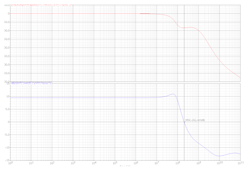
Next we evaluate the closed loop gain, shown in figure 5 and 6. We closed the loop with two
resistors with gain of roughly 10dB based on non-inverting configuration. The phase margin was
roughly 97 degrees, proving the design is stable.
From the simulation result, the DC and low frequency gain was approximately 62dB and the phase margin
was about 100 degrees (-81 degrees at unity gain frequency). The maximum frequency of signal that needs
to be filtered is roughly 500Hz. Hence the 3dB frequency of 5kHz leaves plenty of headroom.

Digital Circuit Design
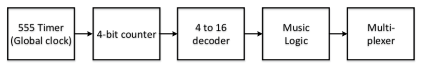
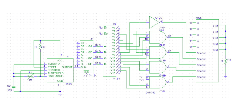
The digital part of the IC was designed to automatically play a short melody demo if started. This function can be triggered by a push button.
An external clock (555 timer) provides clock to the digital circuits. Inside the chip, the first part is a 4-bit counter that increments every
clock cycle. A decoder in the following picks right tones to play in order. Figure 5 shows the block diagram of digital part and Figure 6 illustrates
a detail schematic.
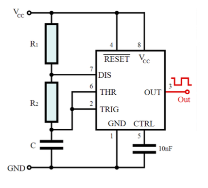
A 555 Timer generates the global clock and since in order to play the legible pitch automatically, we are going
to use the clock frequency about 5Hz, which sets the speed of the auto-play.
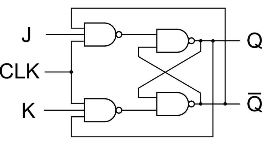
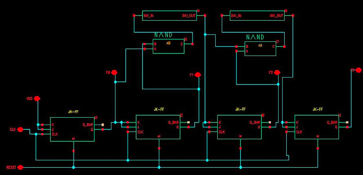
We implemented a JK Flip-flop based synchronous up-down counter. Figure 7 shows a JK Flip-flop cell and Figure 8 shows
how we realized the synchronous up-down counter.
To demonstrate the auto music player, we created a music notation for a song as below.
| Number | 1 | 2 | 3 | 4 | 5 | 6 | 7 | 8 | 9 | 10 | 11 | 12 | 13 | 14 | 15 |
| Pitch | G | E | E | F | D | D | C | D | E | F | G | G | G |
The Finite State Machine is below : output 0: C = 8
output 1: D = 5 and 6 and 9
output 2: E = 1 and 2 and 10
output 3: F = 4 and 11
output 4: G = 0 and 12 and 13 and 14
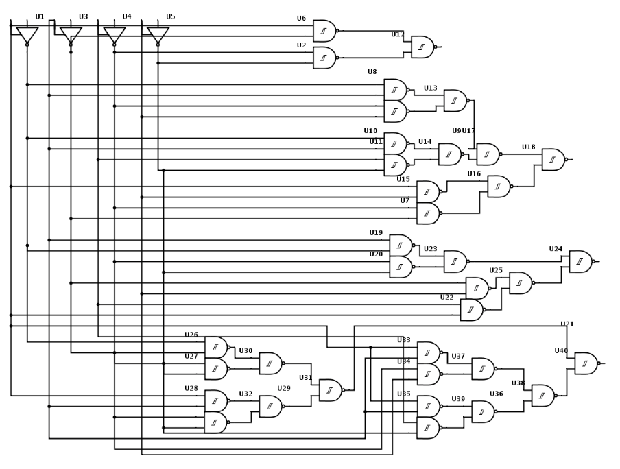
So, after the counter there are some NAND gates and inverters connecting with controller shown in Figure 7 and 8.
The below is the 4 to 16 decoder using the NAND2 gates. The decoder is used to decode the output of the counter
and control the multiplexer to select the pitch in a order of what were shown in the previous table.
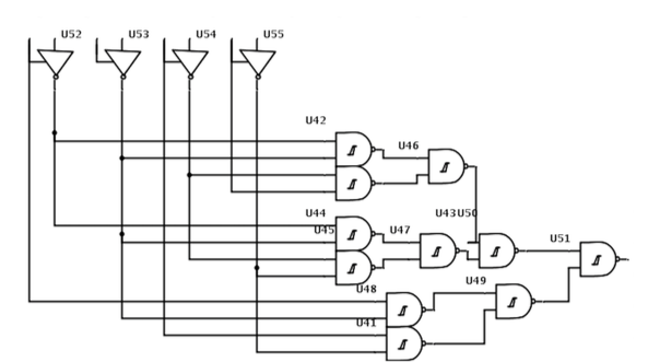
The multiplexer was implemented in the following way:
When cdefg=10000; output = C; cdefg=00010;output = F cdefg=01000;output= D; cdefg=00001;output =G; cdefg = 00100;output =E;
C,D,E,F,G are the pitches which are always oscillated through the amplifiers and 555 Timer, so we let c,d,e,f,g control signals to choose the output.
Therefore, there are five NAND gates to control the output.
Figure 8 shows the schematic for the mux.
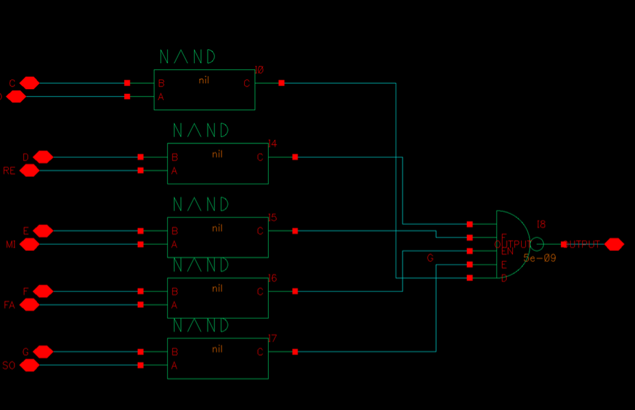
Figure 9 shows the entire system connection in Cadence Virtuoso.
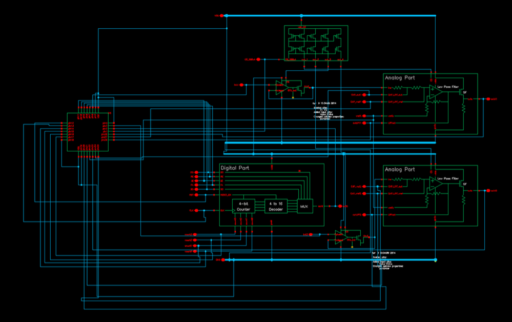
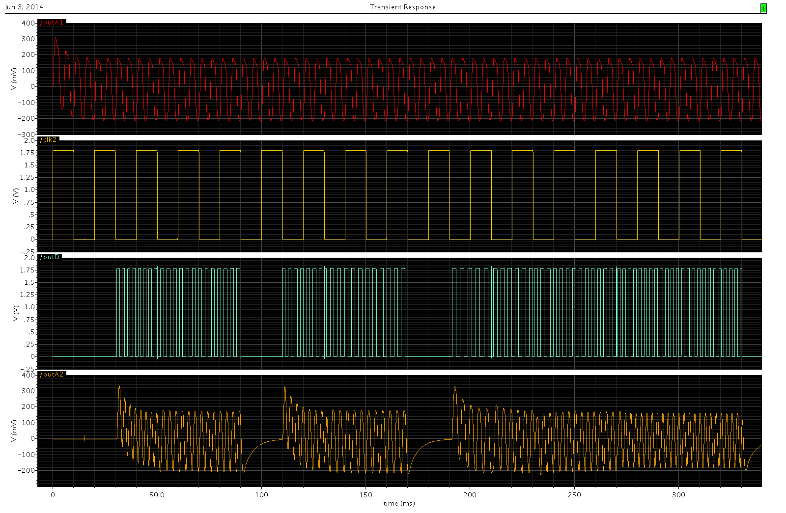
Figure 10 shows the transient response of the IC. We simulated the system by applying a clock and turning on the auto play function.