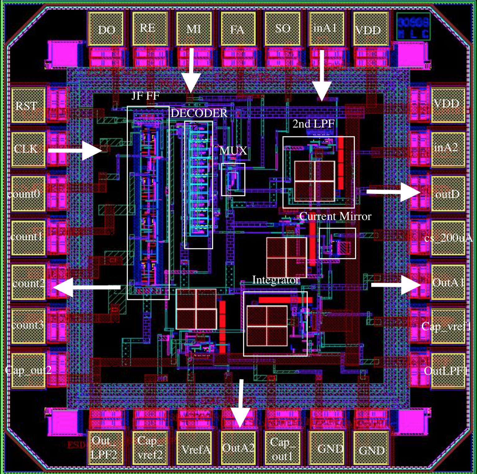
IC Layout
The picture below is the IC layout of the entire design chip. Two pins were used as VDD and two for ground. The blocks were distributed along the die to minimize the trace resistance to the pins, and arranged to follow the signal flow through the system.