
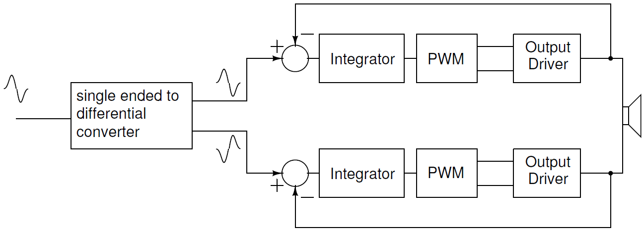
System Design
Input signal frequency range
Since the amplifier is to be used in the audio range, the input is expected to be between 20Hz and 20kHz.
Input signal amplitude
Since this is a closed loop design, the gain of the system is set by the feedback fraction. In this design, we chose the feedback fraction to be 0.5 so that the differential gain of the system is 2. The single-ended to differential converter offers a further "gain" of 2, so that the effective gain of the system from single-ended input to differential output is 4. Since the maximum output amplitude can be $V_{DD}$, the input amplitude needs to be limited to $V_{DD}/4$.
Integrator cut-off frequency
The integrator cut-off frequency needs to be low enough that it rejects spurious tones near the PWM frequency while simultaneously being high enough to let all of the input frequencies pass through unattenuated. In this design, this was set to be 80kHz.
Pulse Width Modulation frequency
The most important consideration while choosing the PWM frequency is the tradeoff between power dissipation and the suppression of high-frequency tones by the loop. As the frequency of the PWM increases, the integrator does a better job of suppressing the spurious tones but since digital power dissipation is proportional to $f C V_{DD}^2$, for a given capacitive load and supply voltage, the power dissipation goes up linearly with frequency. This reduces the efficiency of the system. On the other hand, if the PWM frequency is reduced, the efficiency improves, but now the integrator cannot reject the spurious tones near the PWM frequency as effectively.
The PWM frequency was chosen to be 500kHz. For an integrator cut-off frequency of 80kHz, this offers an attenuation of approximately 16dB at the PWM frequency. We note that in the bridged three-level topology, the nearest spurious tones appear at twice the PWM frequency instead of the PWM frequency itself. Therefore, the spurious tones see an effective 22dB of attenuation in the loop.
Stability analysis
If we model the loop assuming an ideal integrator with a UGB of $\omega_{UGB,int}$ and the PWM and output driver as a block that introduces a delay $\tau$ and a gain of $G_{PWM}$, the loop gain can be written as
\[ L(s) = \dfrac{G_{PWM}e^{-j\omega \tau}\omega_{UGB,int}}{s} \]In our implementation, $G_{PWM} = \dfrac{V_{DD}}{V_{\Delta}}$, $\omega_{UGB,int} = \dfrac{1}{R_{F}C}$. Therefore, the loop gain becomes
\[ L(s) = \dfrac{V_{DD}e^{-j\omega \tau}}{j\omega V_{\Delta} R_F C} \]The loop gain goes to 1 at a frequency of $\dfrac{V_{DD}}{V_{\Delta}R_F C}$. At this frequency, the phase is given by $-\dfrac{\pi}{2} - \dfrac{V_{DD}}{V_{\Delta}R_F C}\tau $. Setting $V_{DD} = 1.8V$, $V_{\Delta} = 0.9V$, $R_{F} = 200k\Omega$ and $C = 20pF$, for a 60$^\circ$ phase margin, we can tolerate a maximum delay of $\tau_{max} = 1\mu s$.
Note that this analysis assumes that the frequency where the loop gain goes to 1 is much smaller than the PWM frequency. In our case, the assumption holds true because the PWM frequency is 500kHz and the loop gain goes to 1 at approximately 80kHz. This assumption lets us write the PWM gain as $\dfrac{V_{DD}}{V_{\Delta}}$. This analysis also assumes that the OTA acts as an ideal op-amp. This will be largely true if the UGB of the OTA is much larger than the frequencies under consideration.