
Block Description
Single-ended to differential converter
The conversion from single-ended signal to differential signal was achieved using 2 OTAs as shown in Figure 1. $R$ in the schematic was chosen to be approximately 10k$\Omega$.

Pulse Width Modulator (PWM)
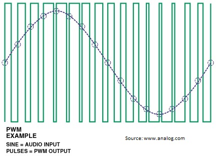
In our design, pulse width modulation is realized by comparing the instantaneous amplitude of an input signal against the instantaneous amplitude of a triangle wave. By making sure that the triangle wave frequency is much higher than the input signal frequency, the output of the aforementioned comparison is a pulse train at the same frequency as the triangle wave. Further, the duty cycle of the pulse train is linearly related to the instantaneous amplitude of the input signal. The typical output of this block is shown in Figure 2.
Triangle wave generator
The triangle wave generator is required in order to realize the pulse width modulation operation. It uses an integrator and a Schmitt trigger as shown in Figure 3. In this case, the peak-to-peak amplitude of the triangle wave becomes $V_{DD}/a$ where '$a$' is set by the resistor ratio shown in the schematic. Also, the time-period of the triangle wave is determined by $R_1$ and $C$ and is given by $4R_1C/a$. In our implementation, we chose $R_1 \approx 100k\Omega$, $R_2 \approx 10k\Omega$, $a=2$ and $C \approx 10pF$ giving a frequency close to 500kHz.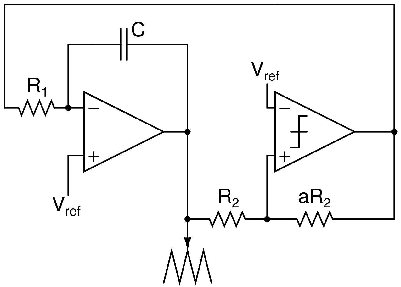
Non-overlap (dead-time) generator
The output driver for a class-D amplifier typically consists of a switch that connects the load to $V_{DD}$ (pull-up) and a switch that connects the load to $V_{SS}$ (pull-down). Here, we define the dead-time as the period during which neither the pull-up nor the pull-down part of the output driver is active. Theoretically, if we had ideal switches, then the dead-time could have been made arbitrarily small. However, given that MOS transistors don't turn off until their $V_{GS}$ drops below $V_{T}$ and that the control signals itself will have a finite slope, we need to introduce some dead time intentionally so as to avoid turning on both pull-up and pull-down networks simultaneously which would effectively short $V_{DD}$ to $V_{SS}$. This would result in a large transient current spike since these devices have very high current carrying capacity, and this might destroy the chip. Further, the amount of dead-time introduced needs to be enough so as to be able to avoid shoot-through currents even in the presence of PVT variations.
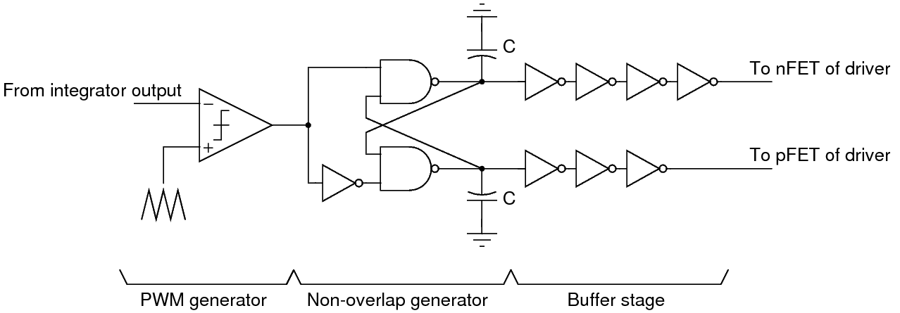
The schematic of the pulse width modulator, the non-overlap generator and the buffers are seen in Figure 4. The digital gates are all standard CMOS structures with $1.8\mu m$ nFETs and $7.2\mu m$ pFETs and minimum length sized appropriately depending on the transistor stack height. $C = 20pF$ is a MIM-capacitor that is responsible for providing the 60ns non-overlap period that we need. Since the waveform at the output of the NAND gate is very slow, we use buffers to improve the ``sharpness'' of this waveform.
Output driver
The schematic of the output driver is shown in Figure 5. The primary consideration while determining the size of these transistors is the desired power efficiency. Let the drop across the load be denoted by $V_{Load}$. Then, the power drawn from the supply is $\dfrac{V_{DD}V_{Load}}{R_{Load}}$ while the power delivered to the load is $\dfrac{V_{Load}^2}{R_{Load}}$. The efficiency is then given by $\dfrac{V_{Load}}{V_{DD}}$. We can see that $V_{DD} - V_{Load}$ is the $V_{DS}$ across the pFET output driver and the nFET output driver of the differential path. Therefore, for a given current through the load, the transistors were sized so that a minimum of 90% efficiency is achieved.
