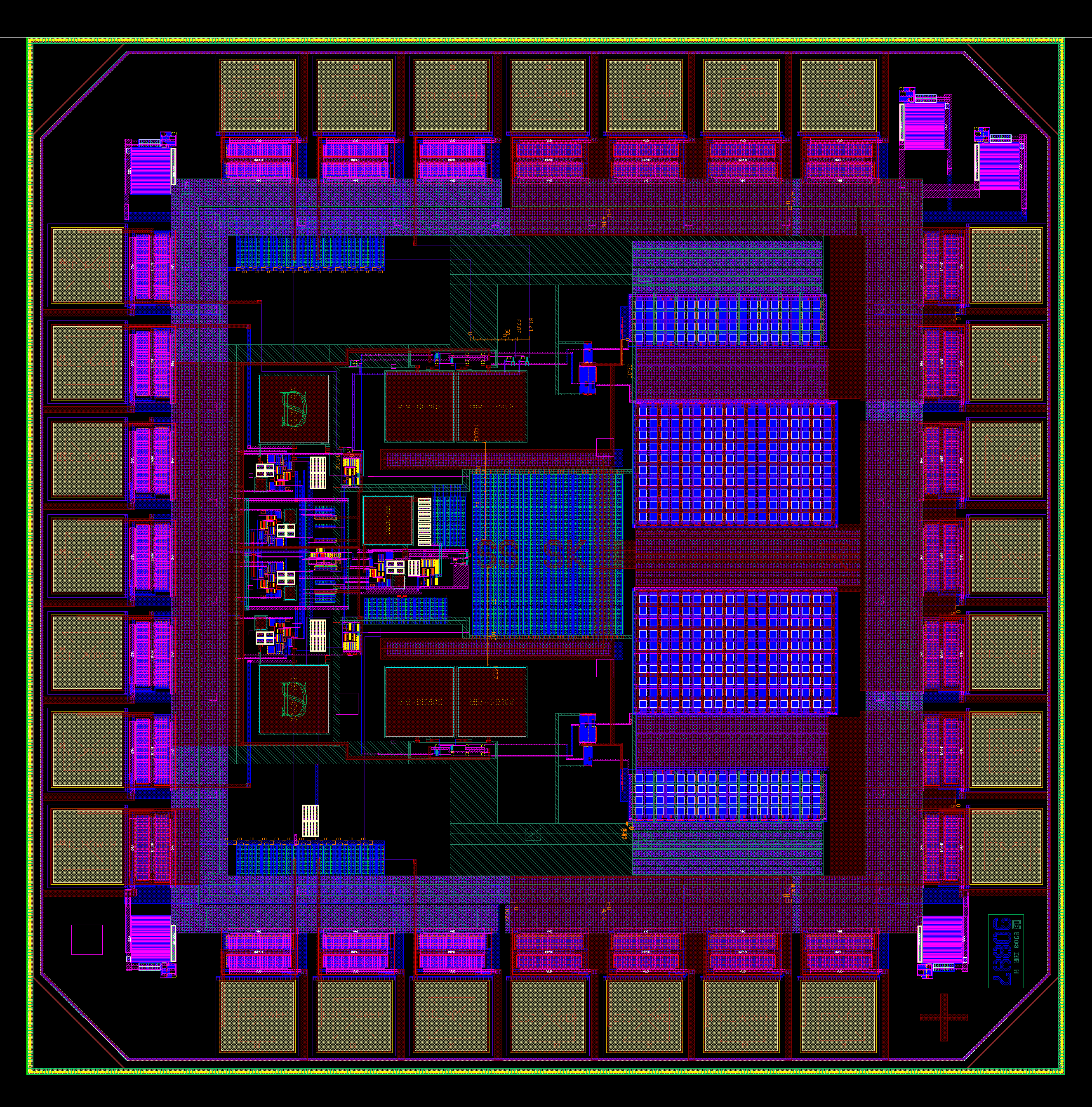
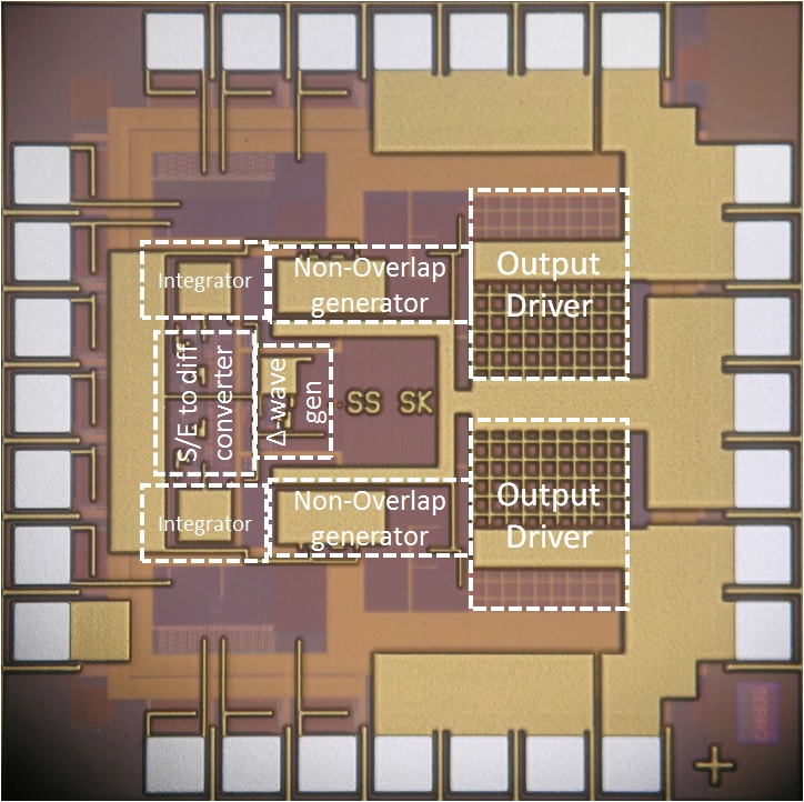
Layout
The design is inherently differential, and the top-level layout reflects this. One half of the circuit was initially laid out and then was copied and mirrored in order to get the differential half. Common blocks like the bias circuit and triangle wave generator are placed along the line of symmetry. The top-level layout is seen in Figure 1. The line of differential symmetry is vertical and cuts across the middle of the chip. The signal enters from the bottom side of the layout and exits from the top. A "+" marker at the bottom-right is used to indicate the location of pin 1 and the required orientation with respect to the package.
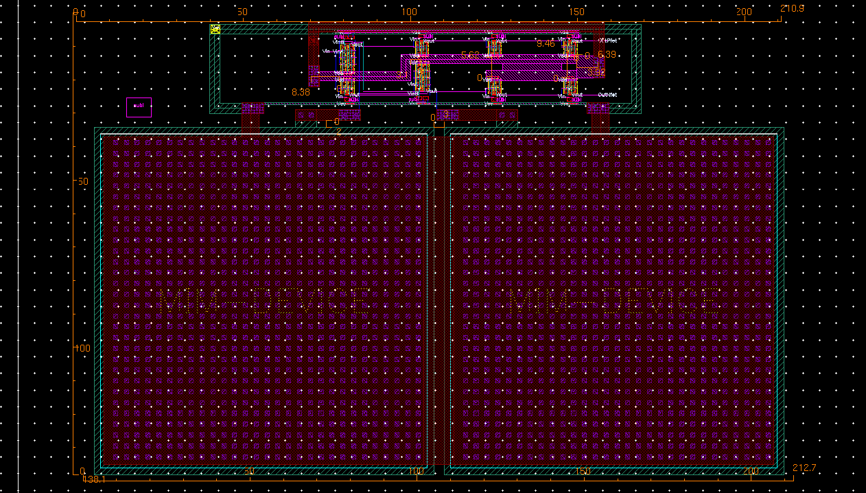
Single-ended to differential converter
The layout of the single-ended to differential converter is shown in Figure 2. This layout was created by mirroring the OTA layout about the X-axis. Care was taken to maintain the differential nature of the design. The $V_{DD}$ and $V_{SS}$ buses run vertically along the left and are tapped off as required to power the OTA blocks.
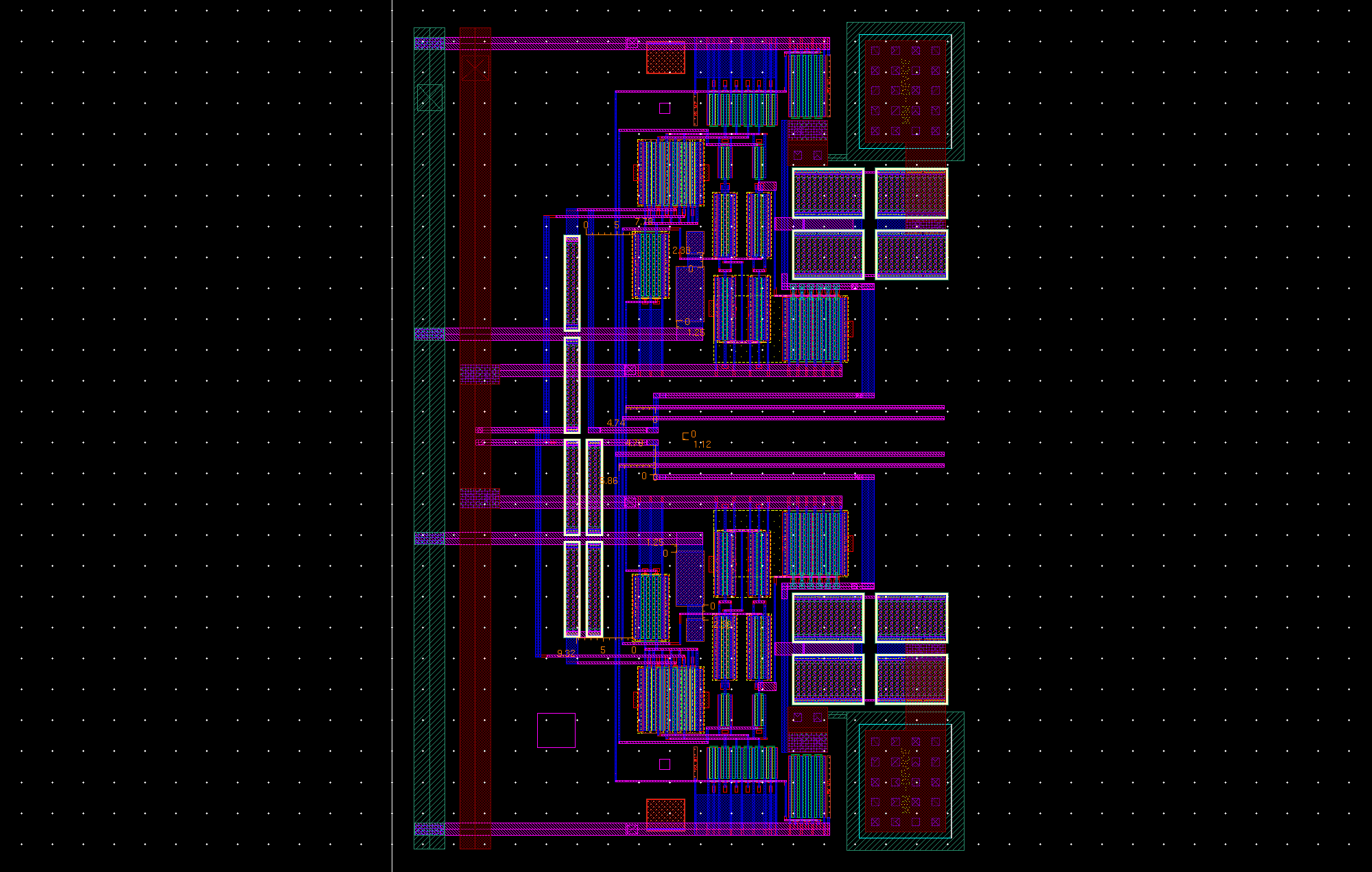
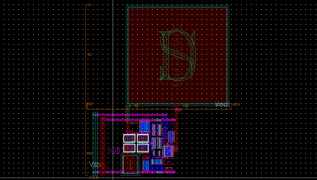
Integrator
The layout of the integrator is shown in Figure 3. The layout is largely dominated by the 20pF MIM capacitor. The $V_{DD}$ and $V_{SS}$ buses run vertically along the left and are tapped off as required to power the OTA.
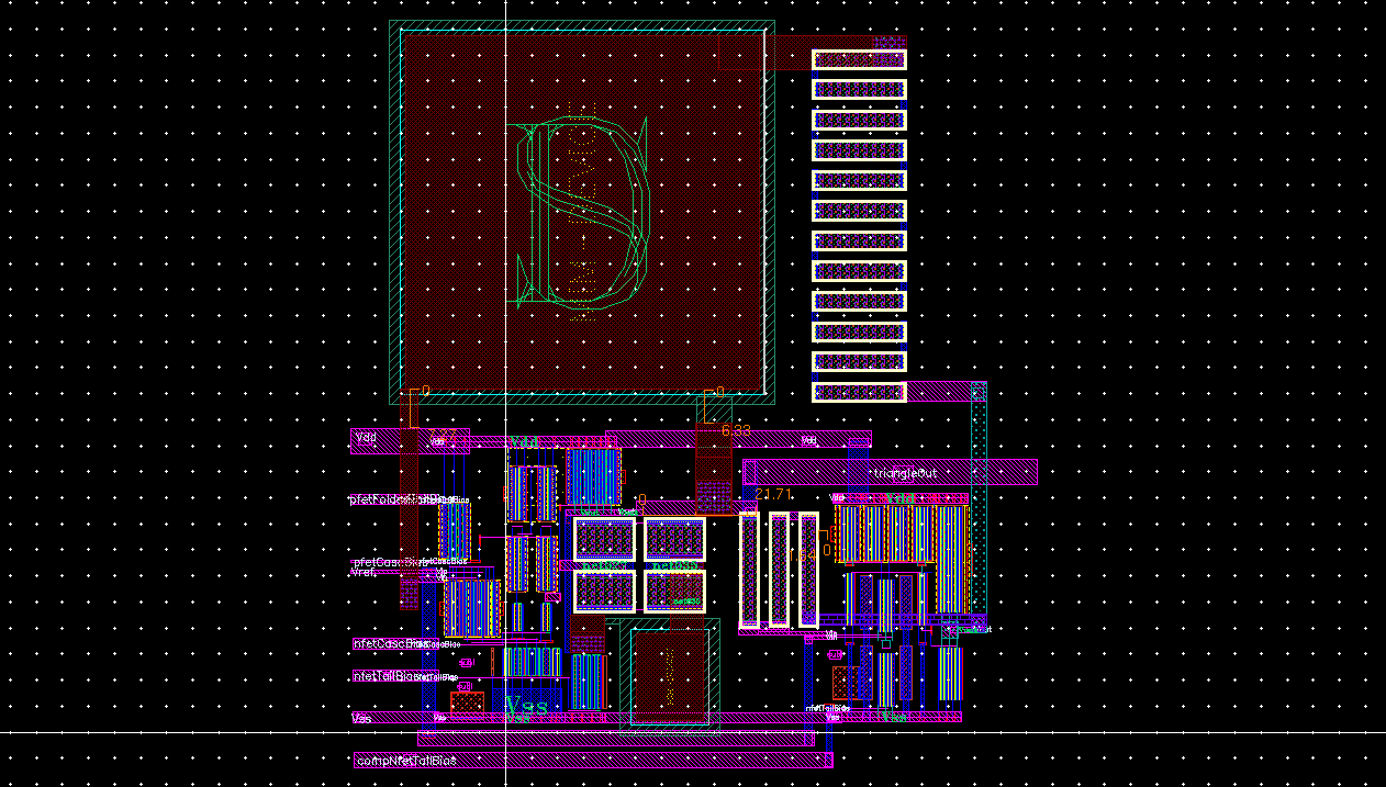
Triangle wave generator
The layout of the triangle wave generator is shown in Figure 4. The resistors '$aR_2$' and '$R_2$' (refer this section) are placed close to each other to improve matching. The large resistor $R_1$ is broken up into 12 pieces and meandered to improve accuracy of the realized value.
Non-overlap generator
The layout of the non-overlap generator can be seen in Figure 5. The layout area is mostly dominated by the MIM capacitors that provide the required delay. The relatively tiny digital gates are all located at the top of the layout in the same order as they appear in the schematic).
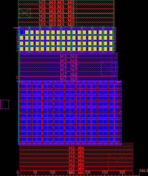
Output driver
The layout of the output drivers is shown in Figure 6. Starting from the top, the layout consists of the $V_{SS}$ bus, the nMOS pull-down, the output bus, the pFET pull-up and the $V_{DD}$ bus. Metal layers are strapped together through the use of via arrays so as to minimize the wiring resistance and to increase the current-carrying capacity of the bus.