
PCB Design
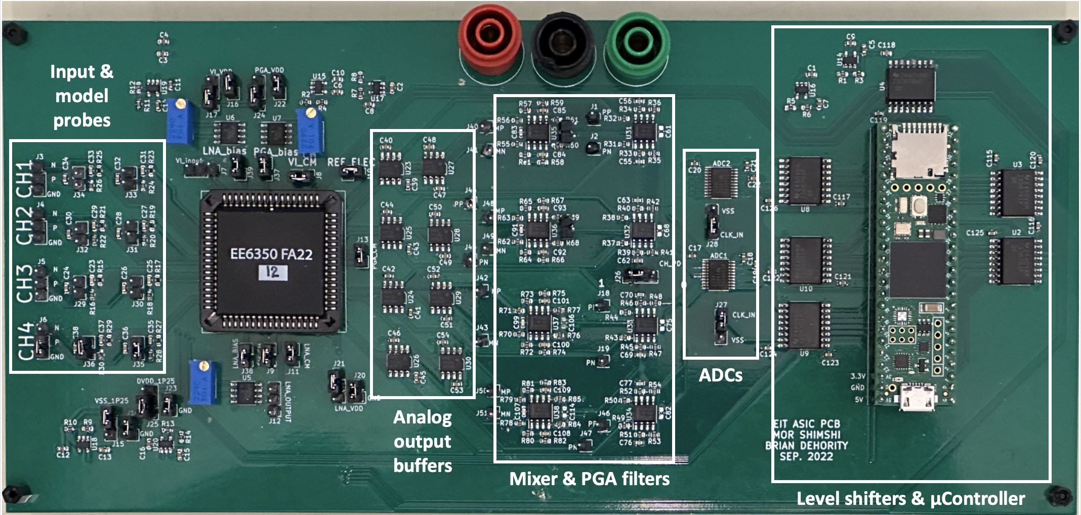
Fully populated PCB - the signal flow is from left to right
The PCB was designed after the completion of the ASIC design. The input for each channel (on the left, labeled CH1, CH2, etc.) is routed to the chip through model electrodes. These circuits, when not shorted, model the probe impedance seen by the chip when it is used with typical EIT electrodes. The analog outputs (PGA and mixer) of the ASIC are buffered, filtered, and sampled. The data from the ADCs is sent to the Teensy, which forwards it to the host computer for processing.