
Circuit Design
Overview
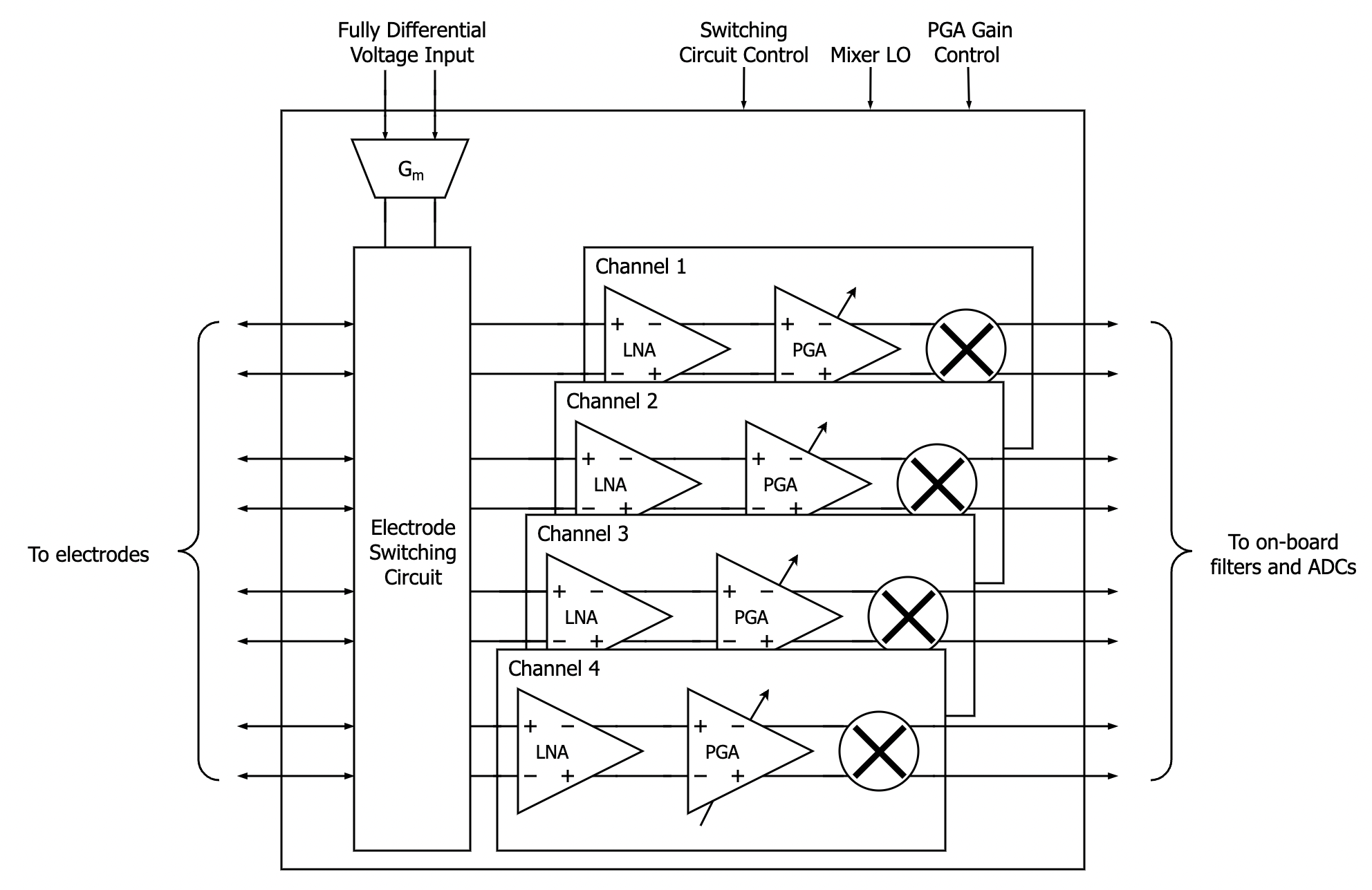
The EIT ASIC was designed and fabricated in TSMC 65nm technology. The 1.1mm x 1.1mm device consists of four channels for voltage recording and a current stimulator. The AC stimulation signal is injected as a current into the material through one of the four channels, and the resulting voltage distribution around the object is recorded by the three others. Each channel consists of a 20 dB fully-differential low noise amplifier (LNA), a fully-differential 0-42 dB (in 6dB steps) programmable gain amplifier (PGA), and a mixer to remove the 1.5 kHz carrier. The device is able to record impedance changes as small as 0.1%, which encapsulates the majority of neural activity that is expected.
Current Stimulator (Gm Cell)
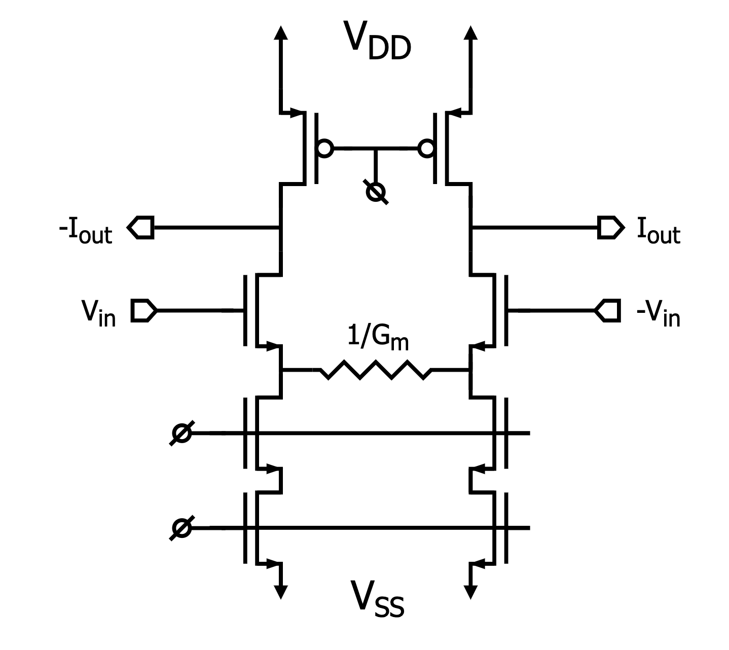
The current stimulator, which is implemented as a Gm cell, receives a fully differential 1Hz - 300kHz AC voltage input between 100mV-1V, and linearly generates a corresponding 1uA - 190uA stimulation current. This current is routed through any two electrodes by the switching circuit (described below), which allows for complete freedom in stimulating the object.
The Gm cell follows the implemention in [4]. The degeneration resistor, alongside the effective gmb resistor from the body effect of the input NFETs, sets the Gm of the complete circuit. The simulated effective Gm is ~180uS. The common-mode feedback circuit (not shown) sets the output common mode through changing the bias of the active load PMOS devices. A cascoded current source is used, due to its improved linearity over the large input range of the Gm cell. The input current bias is routed from off-chip, to allow for greater control over the circuit after tapeout.
Switching Network
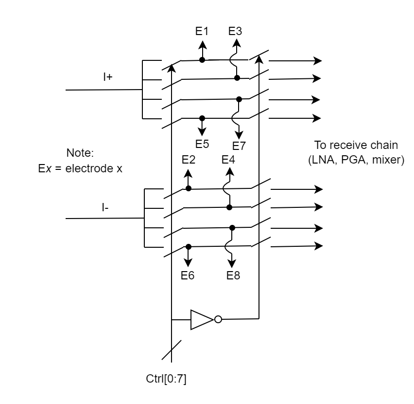
The switching circuit serves two main purposes: to arbitrarily route the current output of the Gm cell to any two electrodes, and to prevent the receive chain from saturating due to the stimulating current on any channel. This is accomplished through two sets of switches. One set shorts any electrode to the current output, and the other opens the LNA input from the electrode. Without the second set of switches, each channel would saturate and clip when stimulation occurred on that channel. The voltages recorded on the stimulating channel would have little to no useful data, as the gm cell would be actively driving those lines, preventing neural data from coupling into the signal.
Low-Noise Amplifier (LNA)
The first stage in our analog front end is a low-noise amplifier (LNA). In our design, we opted to use a fully differential, PMOS input, two stage miller compensated amplifier with an error amplifier for common mode feedback to ensure stability and reduce DC offset. In order to avoid DC coupling, we use capacitive feedback to achieve 20dB of gain in our pass band, which also allows us to set our high-pass corner using a parallel feedback resistor. In order to achieve a high pass corner that does not attenuate signals of interest around our carrier, we employ pseudo resistors in the form of reverse biased PMOS diodes. This allows us to set a high pass corner of roughly 3Hz. The total power consumption of this block is less than 175uW.
Programmable-Gain Amplifier (PGA)
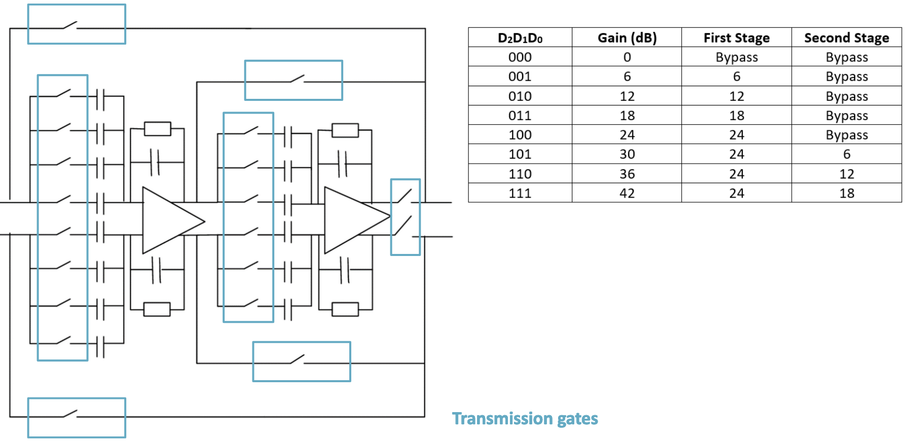
The programmable gain amplifier follows the LNA to provide more amplification. It is needed due to the wide dynamic range of the voltage input coming from the system being measured. The gain can be digitally programmed using 3 bits from 0dB (bypass) to 42dB (1x to 128x). The PGA consists of 2 gain stages with max gain of 24dB and 18dB respectively. Each gain stage uses a two-stage amplifier architecture with Miller compensation. PMOS pseudo-resistors were used in the closed-loop feedback path to provide high resistance (hundreds of GΩ) to achieve a high-pass cut off frequency at ~10Hz. Capacitive coupling was used at the input to reject any DC signal. The ratio of this input capacitance to feedback capacitance is used to set the closed-loop gain. At each gain level, different combinations of input capacitors can be selected to set the gain using complementary switches.
Mixer

The mixer takes two inputs, the received amplitude modulated 1.5kHz carrier (RF), and a 1.5kHz square wave local oscillator (LO). The LO inverts every half wave of the received signal. This ultimately serves to mix the two frequencies, and the resulting output is measured on the IF port. The modulated signal, near but not directly at 1.5 kHz, will be brought down to baseband by this mixing, after which the carrier can be filtered out, leaving only the data from the neural signal or resistive shift.