
Layout Design
The layout design was split into two primary "phases" - the layout of the individual blocks and channel, then the layout of the top-level.
Channel Layout
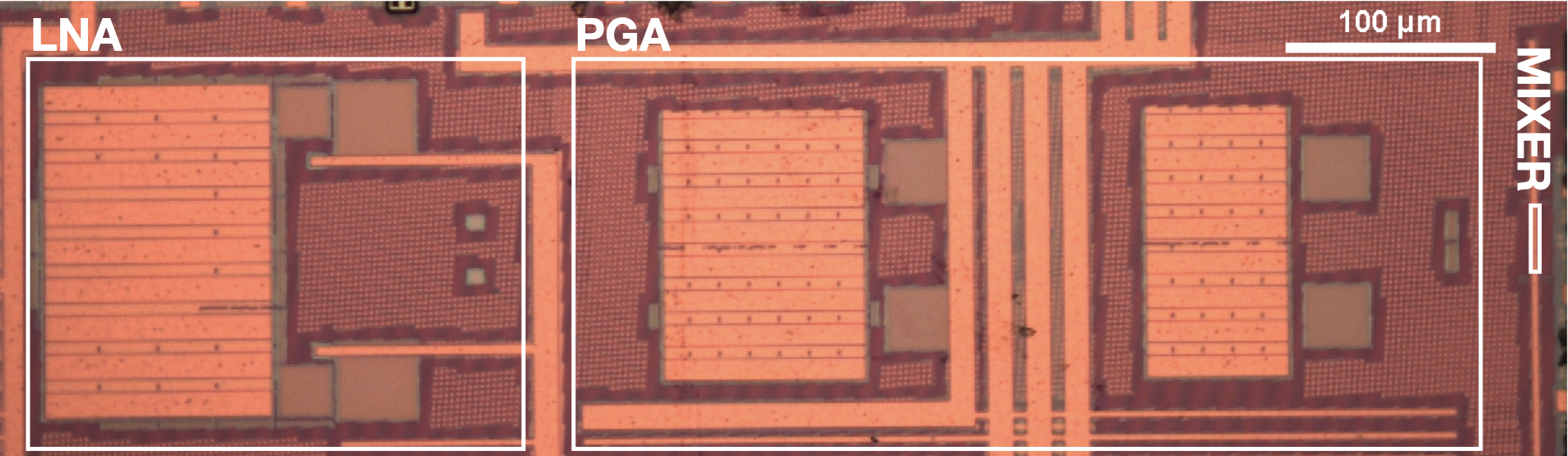
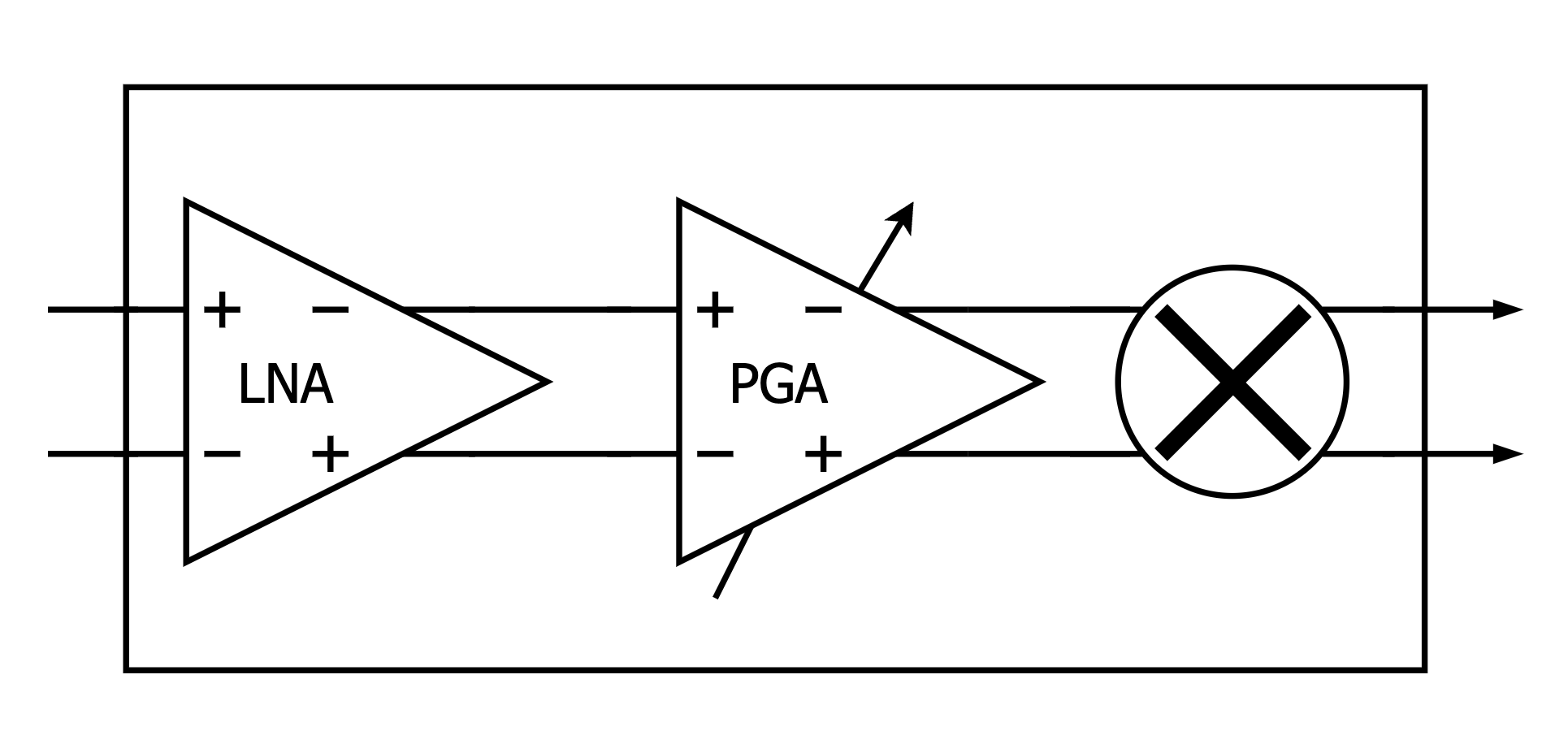
The channel layout is analogous to the block diagram of the channel. The signal flows from left to right (coming from the electrode switching circuit). After amplification (LNA and PGA) the signal is routed to the mixer, then off-chip.
The channel was designed so an identical copy could be used for each of the four channels, which can be seen in the figure below. This enables both better matching between the channels, as well as less re-work for each channel. The LNA and PGA use capacitive feedback, thus capacitor banks were used for better matching. All capacitors were metal-oxide-metal (MOM) capacitors.
Top-Level Layout
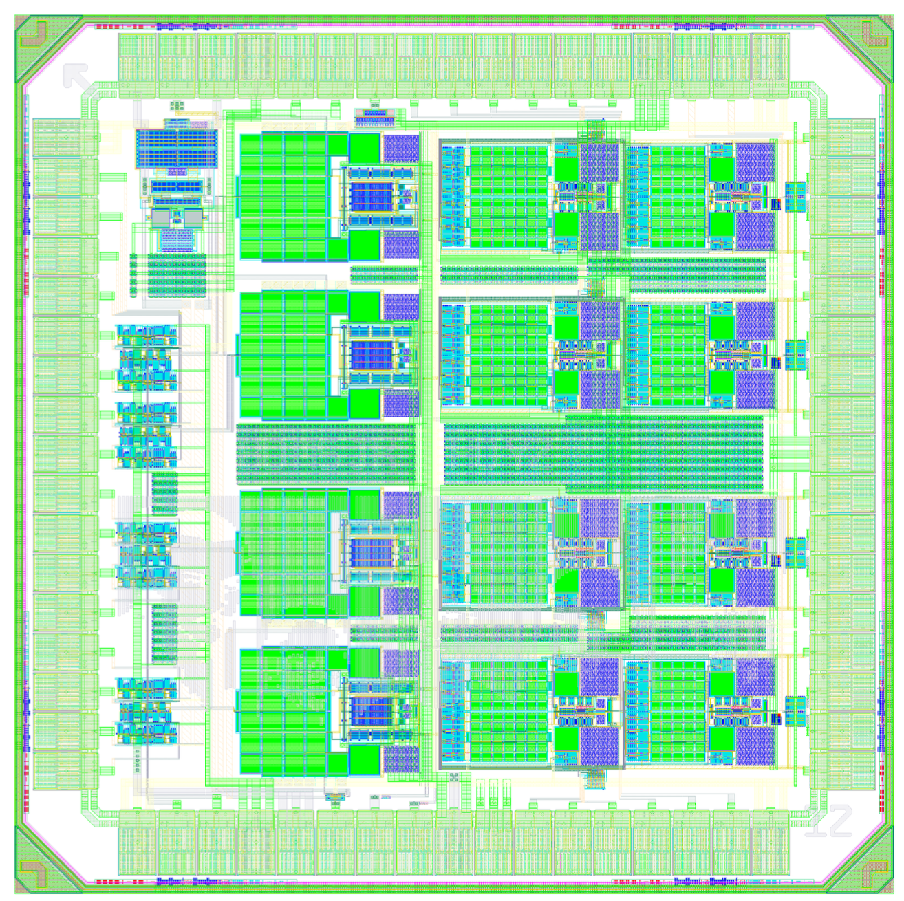
The top level layout was designed concurrently with the channel layout. This approach enabled us to leave space between the blocks in each channel, so that top level routing could be done effieciently. The current biases for each block are also routed between the amplifiers.
The channels are mirrored around the center of the chip, allowing for the same output routing structure to be used for all of the channels. The electrode switching circuit is placed near the input pads, so the routing can be minimalized for lower series resistance. The Gm cell was placed at the top left of the chip so routing the output current signals to the switching circuit was efficient.
The Gm cell and switching network can be seen on the left-hand side of the chip. These were placed near each other to limit parasitics.
After the complete layout was completed and LVS clean, MOS decoupling capacitors were
added throughout the chip.