PCB Design Overview
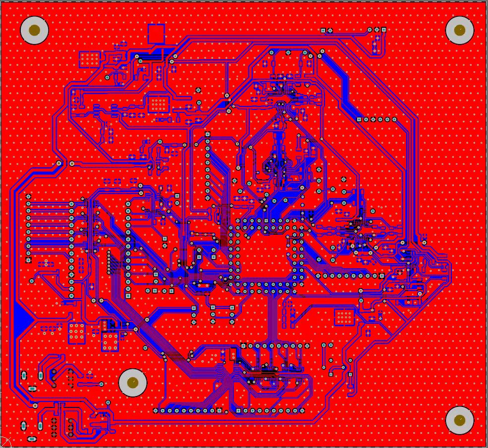
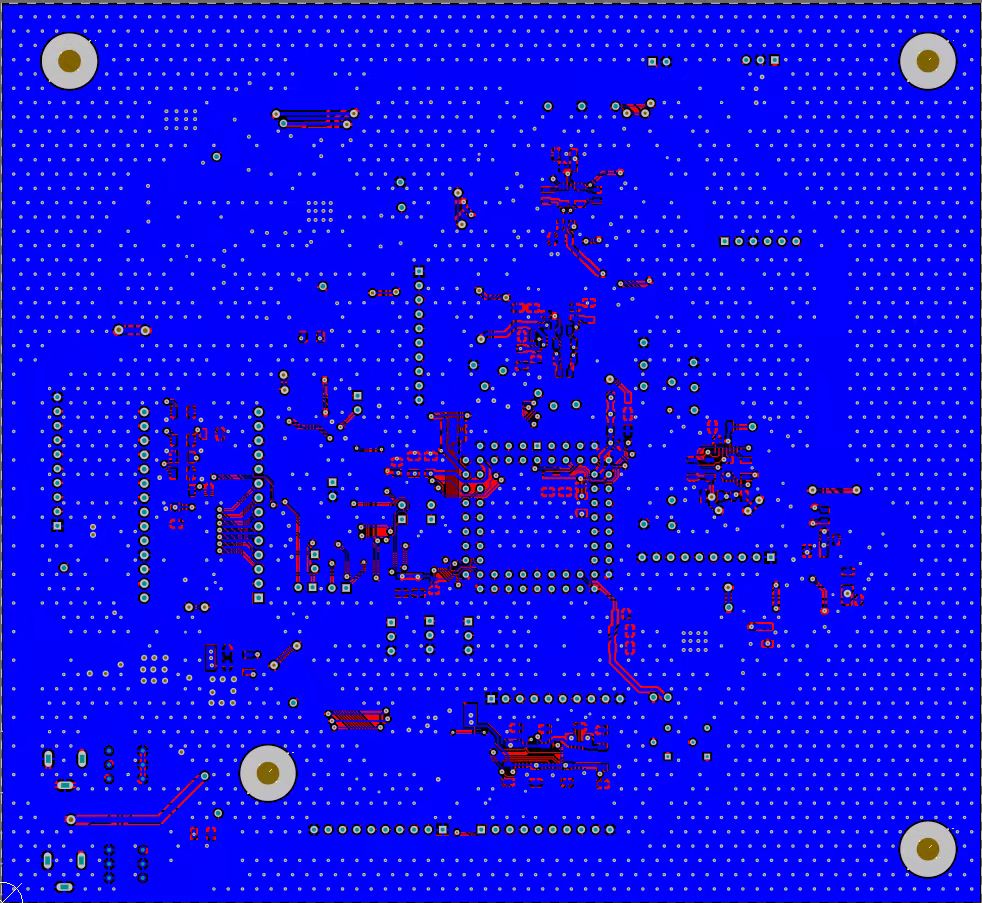
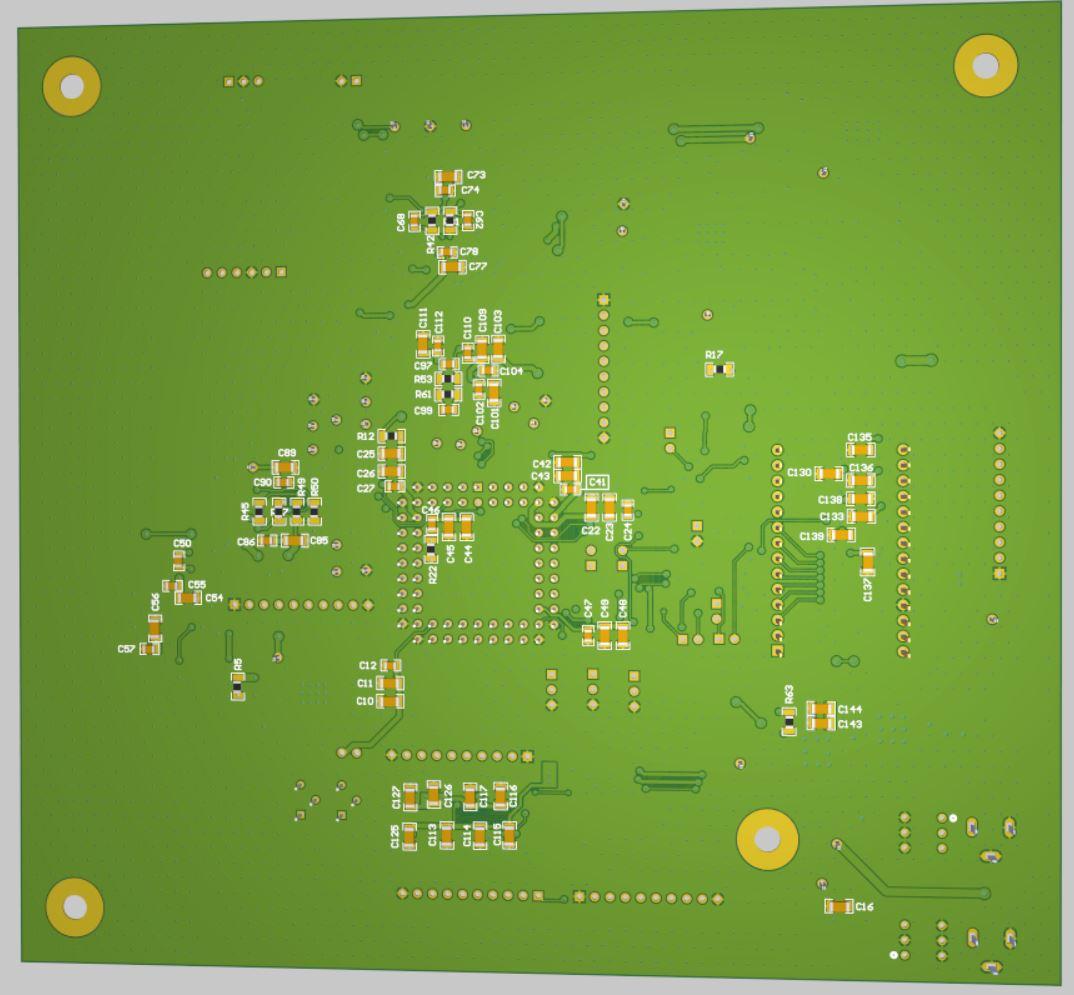
The PCB is designed to accommodate the FMCW Radar module, FPGA, LDOs, Buffer Amplifiers, and Low Pass. The board has a two-layer stack-up with a clear ground layer to ensure a good ground connection for all chips on-board.
The signal from the radar is pre-amplified before going into the mixer on-chip. The LO for the downconversion of the RF is routed from within the FPGA. The frequency modulation is enabled by the VCO on board the Radar module. The VCO receives its signal from a Current-Steering DAC. The current signal from the DAC is routed to an external TIA block before going to the radar’s VCO. This enables external tunning of the modulator voltage. The dedicated digital section on-board enables the voltage level shifting and the serialization of communication between the chip and the FPGA.
The board hosts several LDOs that provide both positive and negative voltage capabilities (6V, 2.5V, 1V, -1.5V). The LDOs are both low noise and low Iq. With the low Iq LDOs, the board can work for extended periods of time when running on a battery. The board also hosts low noise voltage and current references for the dual 8-bit differential ADC and other analog circuitry on-chip.
The PCB layout was done in Altium Designer. The digital and analog blocks were placed far apart from each other with a single solid ground layer. The return currents for the signals were mapped to ensure there was no crisscrossing or mixing. Critical tracks are made short with fewer vias or layer transitions. A ground pour was also placed on the top layer and both layers were stitched with vias to reduce any potential interference and to ensure good return paths.