
IC Design
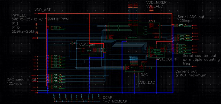
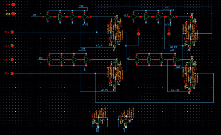
Mixer
The mixer will multiply the input signal with the sweeping LO signal and downconvert the corresponding frequency component to DC. If there are multiple frequency tones within the baseband signal, they might be incorrectly converted to the DC by multiplying them with the harmonics of the mixer signal. So we need to implement a harmonic rejection mixer.
Several topologies of mixers were evaluated (single, double, and passive switch). Due to the limited voltage headroom of this technology (1V), we chose to use the double-balanced switching mixer as the structure. However, the switching process by itself is inherently distorted because of the usage of square waves which contain all the odd harmonics of the fundamental tone. Thus a pulse width modulated LO signal is used with all the switching processes happening at a much higher frequency (300 kHz PWM carrier) and modulates a pure sine wave at the band of interest. The sine wave is sweeping from 500 Hz to 25 kHz in the period of 500 ms.
8-bit Current-Steering DAC
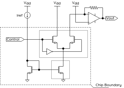
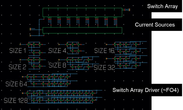
An 8-bit current steering DAC with 125 ksps sampling rate is designed to generate the modulation signal. The current steering DAC is the preferred architecture for high-bandwidth converters. This architecture works by summing the current produced by an array of current sources. We wish to convert an 8-bit digital signal, Din, to an analog current, Iout. Each input bit controls a current that is binarily weighted with respect to a unit value, Iu. Here, D1 denotes the least significant bit (LSB) and DN the most significant bit (MSB). The current sources are scaled up by a factor of two from one bit to the next, yielding

An off-chip TIA is used to convert the current to voltage and drive the VCO in the radar module.
8-bit SAR ADC
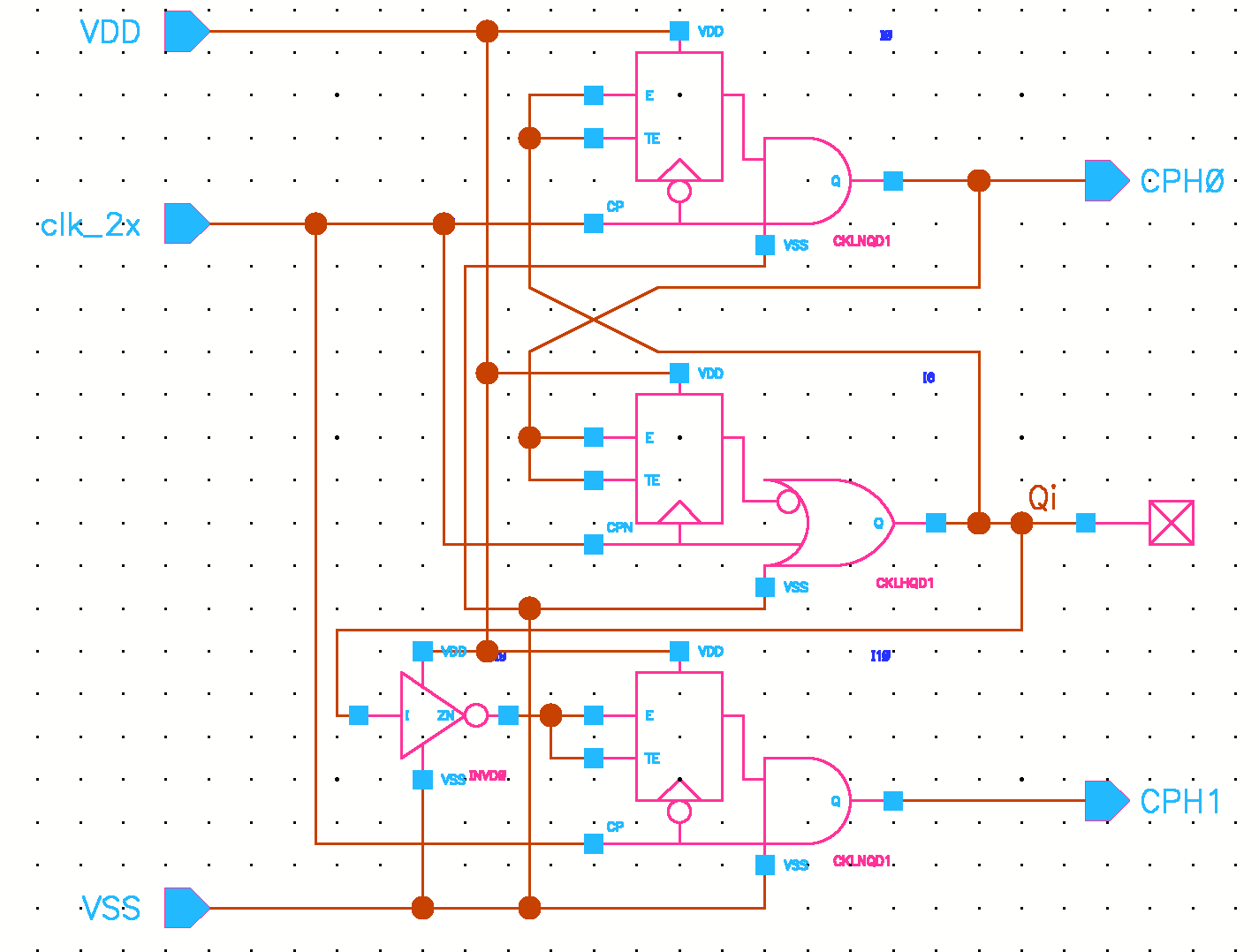
A fully differential 8-bit SAR ADC with 125 ksps sampling rate is designed to sample the downconverted signal. SAR ADC applies the binary search algorithm in a feedback system to produce a digitized sample of data after a series of sequential iterations. It mainly consists of an internal clock generator, bootstrapped sample and hold switch, binary-weighted charge redistribution capacitive DAC, StrongArm comparator, and SAR logic. In an 8-bit SAR ADC, the conversion operation consists of 3 main processes: sample & hold, comparison for 8 times, and then generating the digital code. An extra serializer implemented as an 8-bit shift register is used to serialize the parallel bits and send them back to the FPGA.
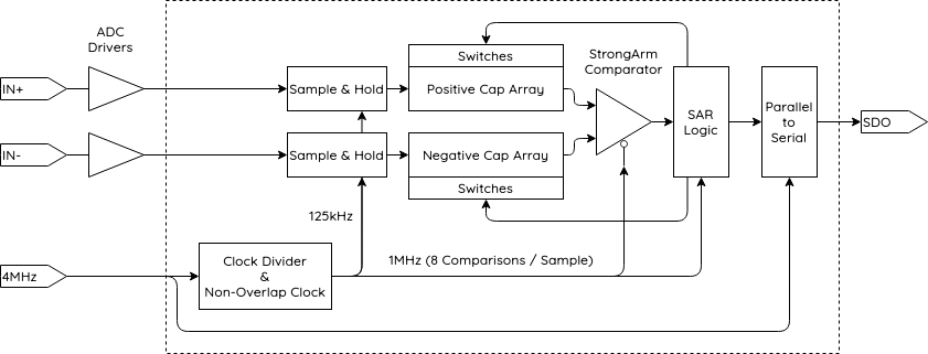
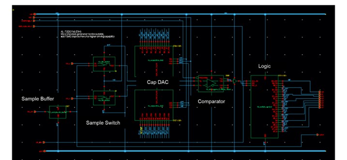
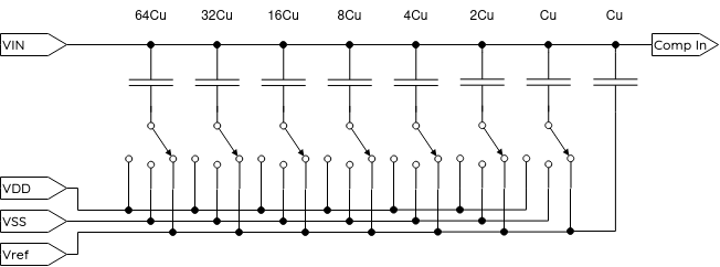
The Capacitive DAC is responsible for converting the digital code coming from the SAR logic into the corresponding analog voltage level to be compared by the comparator. Top plate sampling is used.
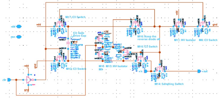
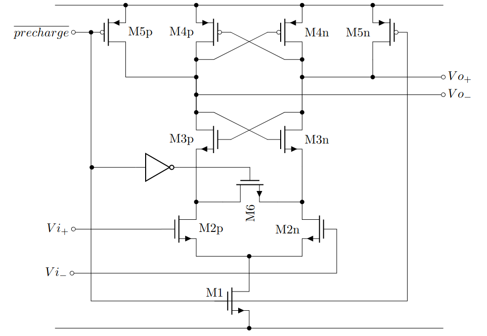
A sample and hold circuit is implemented with bootstrapped switches, which are used for low non-linearities.
The comparator's function is to compare the analog input levels coming from the DAC and generate a digital output bit to control the SAR logic and thus control the switch array.
Zero-Crossing Counter
The zero-crossing counter is a synthesized digital module for doppler-mode operation. In essence, it is a digital counter that runs on the 4MHz clock. The idea is to obtain the fundamental frequency of the incoming signal by counting the number of clock cycles between zero-crossing points. With the assumption that the frequency of the local clock (4MHz clock) is known, the incoming frequency can be calculated using the counts.