
Testing
We followed a systematic procedure to test the functionality and performance of our IC. When we obtained the IC and PCB, we first verified visually whether the bonding wires connecting the packaging and the IC die were of good quality. Meanwhile, we verified that all four voltage regulators on the PCB give accurate and stable voltages. Also, we adjusted the potentiometers on the PCB to tentative values that we used on breadboard. Upon knowing that the connections were good, we proceeded to connecting the IC to the PCB to test the IC’s DC operating points and whether the bias currents were within the expected range of around 20uA.
For the functionality test, we first applied a 1Hz, 5mV peak-to-peak sinusoidal signal to the input. For the OTAs, we set each of their gains to 50, and measured at the output of each expecting an amplified signal with the same frequency. Figures 18 to 20 show the input signal, first OTA’s output, and second OTA’s output respectively. We also changed the gains and the input signal for a more thorough testing. The first OTA outputs waveform with approximately 250mV peak-to-peak, while the second OTA’s output swings from rail to rail because its input was effectively 250mV from the first OTA.
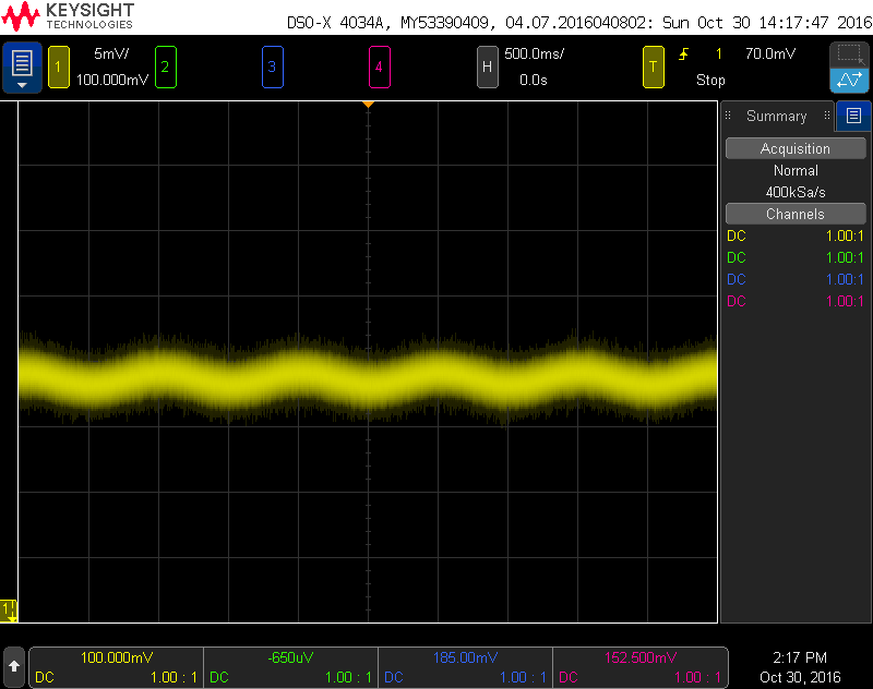
Figure 18. Sinusoidal input signal
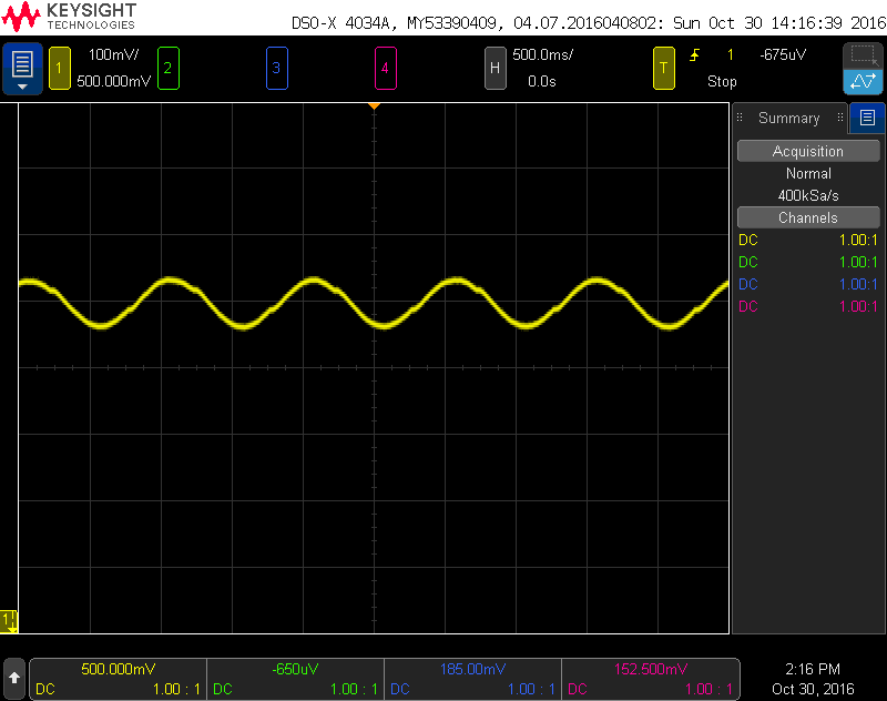
Figure 19. First OTA output with sinusoidal input
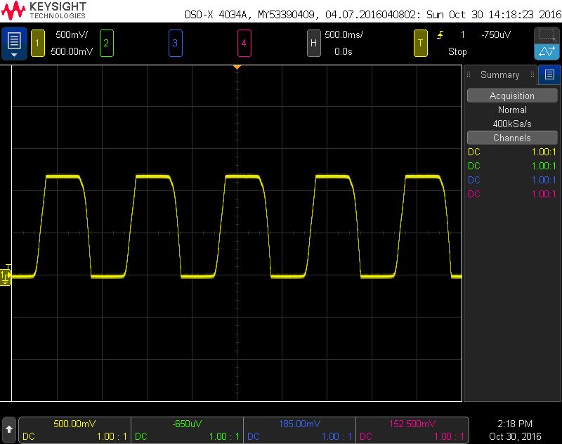
Figure 20. Second OTA output with sinusoidal input
For the comparator, we set the threshold voltage to 0.8V and applied a 1Hz, 600mV peak-to-peak sinusoidal signal with the DC point around 600mV, and we measured at the comparator’s output expecting a square-wave signal with the same frequency as the input signal. Figure 21 shows the result of this testing. We also applied a sinusoidal signal about the threshold value to show that the hysteresis value is indeed approximately 50mV.
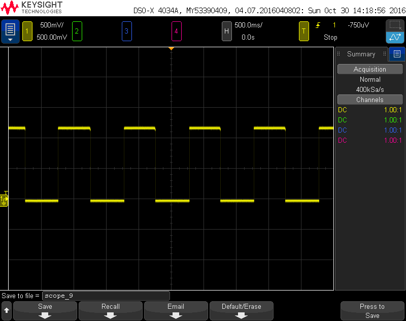
Figure 21. Comparator output with sinusoidal input
After testing each block with a sinusoidal input, we applied a real PPG signal acquired from the Oximax sensor to the first OTA’s output, and measured the voltage at the comparator output. Figures 22 to 25 show input PPG signal, first OTA’s output, second OTA’s output, and the comparator output respectively. Notice that the input PPG signal was several times smaller in magnitude than the 5mV peak-to-peak test signal before, and was also noisier. However the system still outputs the correct heart rate at the comparator’s output.
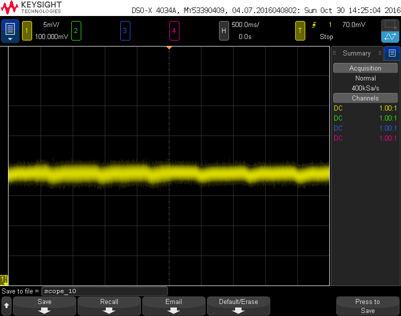
Figure 22. PPG input signal
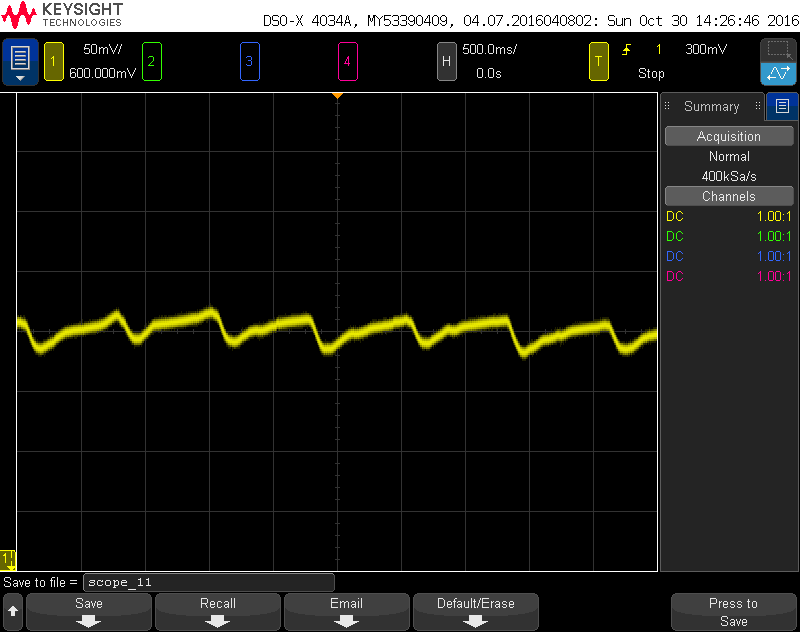
Figure 23. First OTA output with PPG input
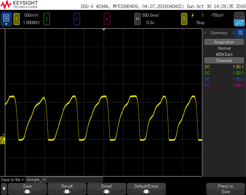
Figure 24. Second OTA output with PPG input
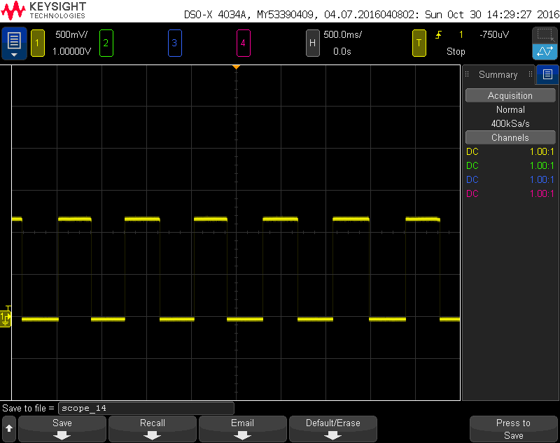
Figure 25. Comparator output with PPG input
Figure 26 shows an example of the LCD displaying a measured heart rate of 84 beats per minute (BPM). Our PCB also supports installing the Arduino and LCD on the board itself.
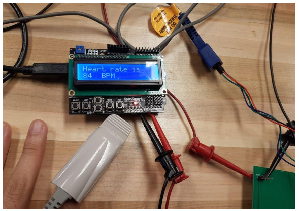
Figure 26. LCD showing heart rate