
Component Design
OTA Design
For the OTA, we choose a differential topology that offers high gain, large output swing, and enough bandwidth to accommodate for the frequency range we are interested in, which is less than 5Hz. The output voltage range is given by the expression VOV to VDD - VOV. The reason we choose NMOS differential pair is because NMOS transistors have approximately 3 to 5 times higher mobility than PMOS counterparts, translating to higher trans-conductance. Figure 5 shows what the OTA consists of. This is also roughly how we lay out the OTA. Figure 6 shows the OTA schematic.
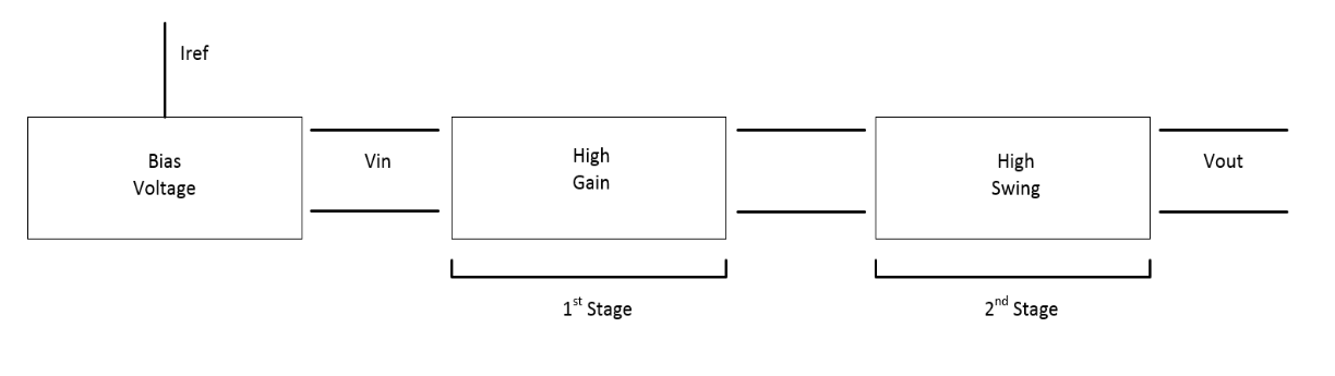
Figure 5. OTA stages
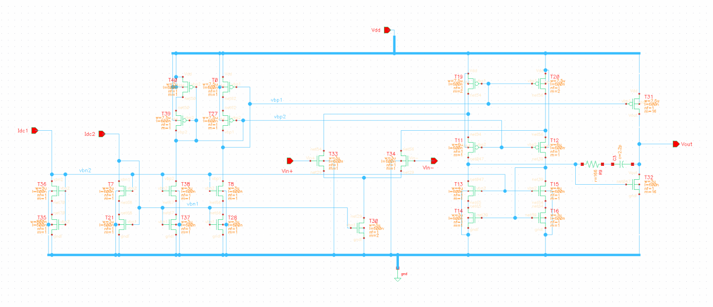
Figure 6. OTA schematic
Figure 7 shows the open loop simulation for the OTA. A list of important results from the simulation: low frequency gain is 73 dB, 3dB bandwidth is 1.3 KHz, and unity gain bandwidth is 18.4 MHz.
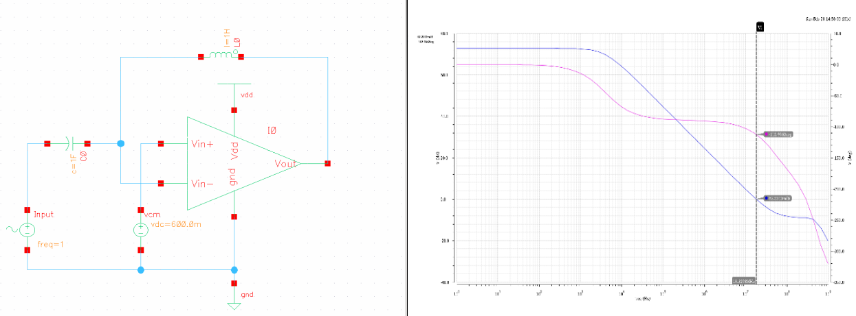
Figure 7. Open loop simulation for OTA
Figure 8 shows the OTA loop gain simulation and result with load impedance. The loop phase margin is simulated to be 80.1 degrees using "stb" analysis.
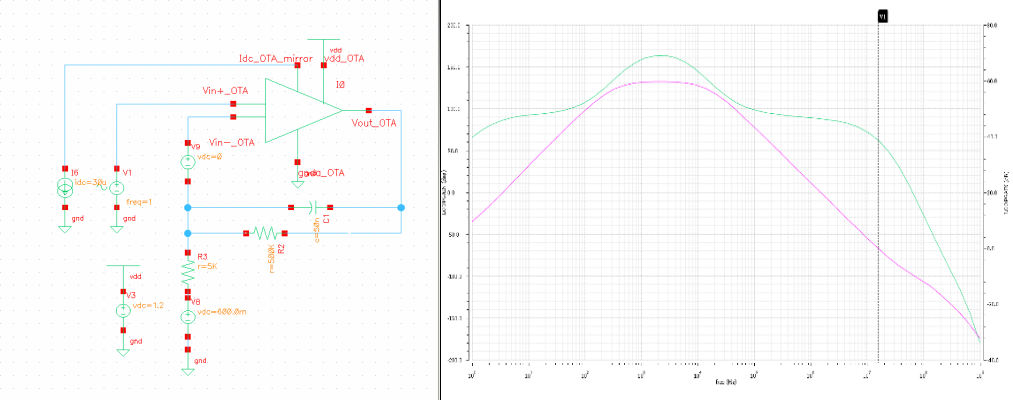
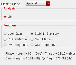
Figure 8. OTA loop gain simulation
Figure 9 shows the PVT results for the OTA’s closed loop response. At DC, the OTA gain differs by about 4dB between the extreme corners.
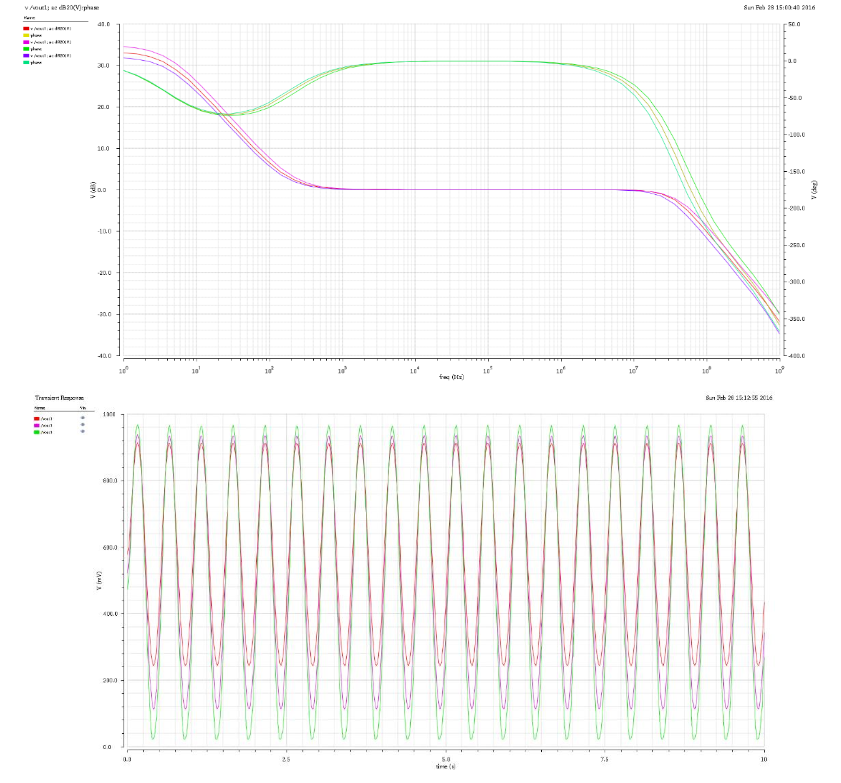
Figure 9. OTA closed loop PVT results
Figure 10 is the simulation result for the OTA’s step response, with the slew rate measured to be 3.62 V/ms. This slew rate is acceptable because we only detect the rising edge of each pulse. As long as the slew rate is consistent across pulses, our measurement will be not greatly affected.
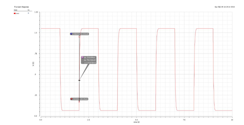
Figure 10. OTA step response
Comparator Design
The comparator in our system is used to convert amplified PPG signal into rail-to-rail square waves that will be easily recognized by the Arduino that processes that signal. Due to the noise present in the input signal, the comparator that we design includes intrinsic hysteresis to combat. Without the built-in hysteresis, the comparator may have the tendency to output erroneous binary states if the input signal happens to swing up and down about the threshold. With the hysteresis, the signal needs to pass two thresholds in order for the comparator output to the change state. The hysteresis of the comparator is 50mV, and the threshold is set by the reference voltage to be 0.8V. The system has the flexibility to readjust the reference voltage, in order to deal with situations where even the amplified signal does not reach the threshold at all. Figure 11 shows a schematic of the comparator.
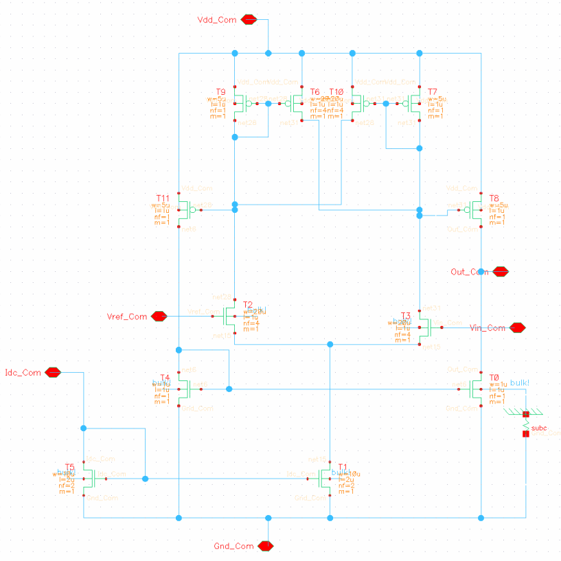
Figure 11. Comparator schematic
Figure 12 shows the comparator’s simulated output given a sinusoidal input that crosses the threshold set at 0.8V.
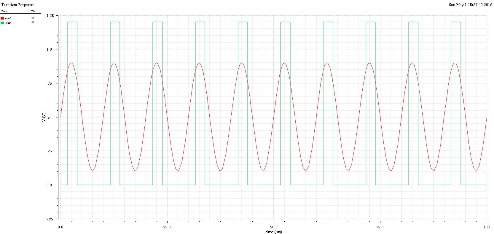
Figure 12. Comparator output