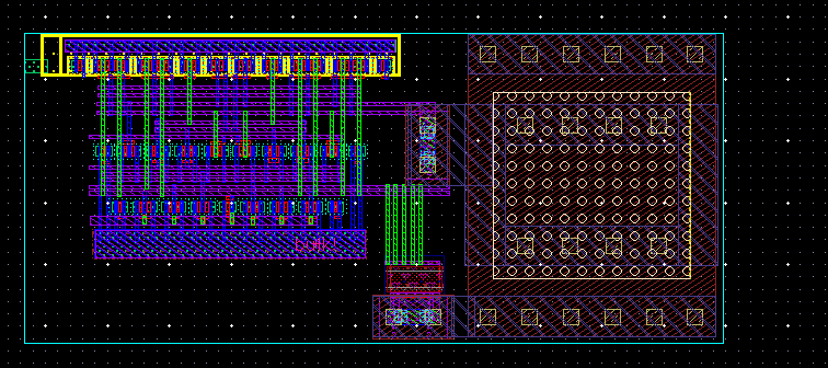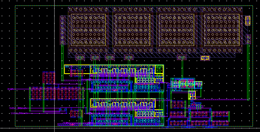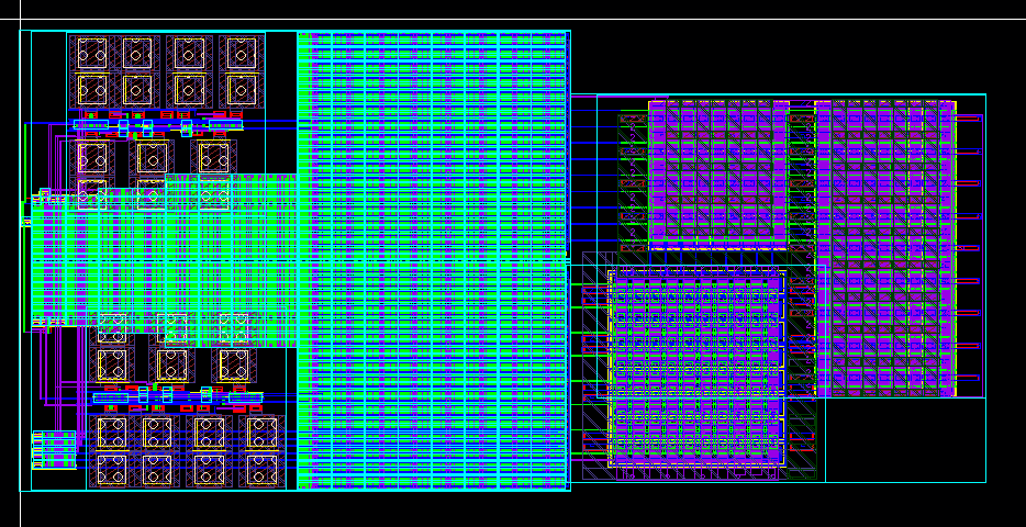
LAYOUT
Layout started with design of output drivers because of stringent ESD requirements. Drain of mosfet connecting the output pad required guard ring, so a lot of effort went into
laying out the output drivers. The design is inherently differential, and the top-level layout reflects this. One half of the circuit was initially laid out and then was copied
and mirrored in order to get the differential half. Common blocks like the bias circuit and triangle wave generator are placed along the line of symmetry.
The top-level layout is seen in Figure 1
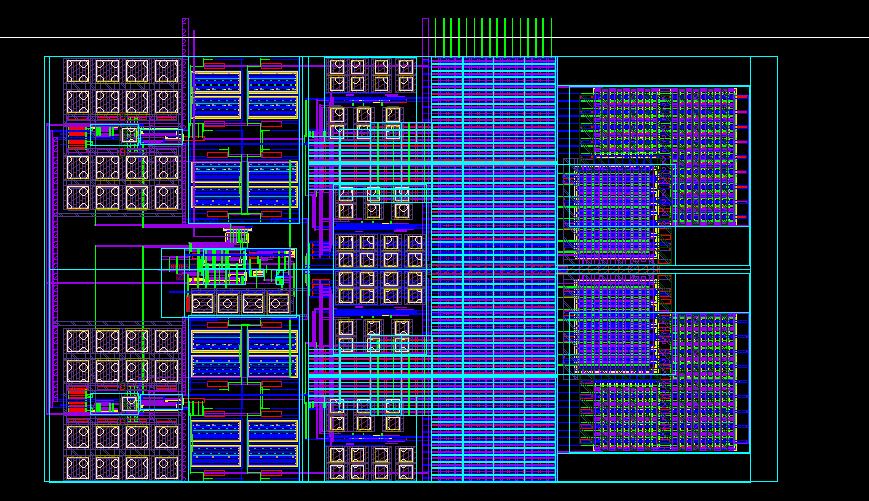
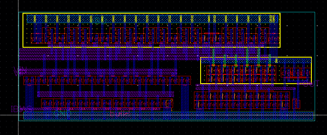
The common centroid layout technique describes that if there are n blocks which are to be matched then the blocks are arranged symmetrically around the common centre at equal distances from the centre. This technique offers best matching for devices as it helps in avoiding cross-chip gradients. Opamp input and mirror-loads are matched using common-centroid technique and dummy trasnsistors are placed on the extreme ends in order to minimize edge effects.