
BLOCK DESCRIPTION
System Design:
The IC comprises the following critical blocks:
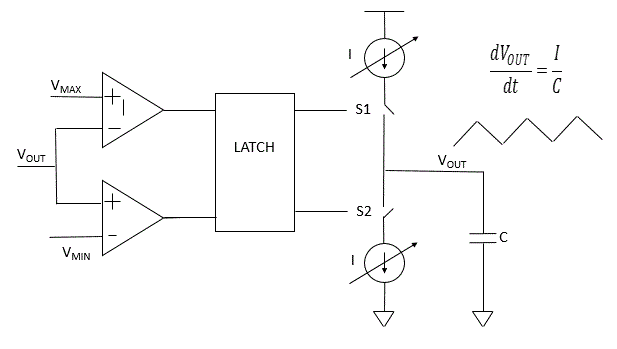
1. Triangle wave generator
This is a relaxation oscillator that generates the triangular wave used in translation of input wave to pulse-width modulated wave. A tunable charge pump charges and
discharges based on the switch states. The slew rate of charging or discharging is given by I/C. The trip points between charging and discharging are determined continuously
comparing the voltage on the capacitor with maximum and minimum swing limits. Keeping C fixed, the switching frequency can be controlled by the magnitude of current.
The voltage across the capacitor thus gives a free-running triangle wave.
2. Operational transconductance amplifer
Operational amplifier is used as an integrator, providing a low pass filter action. Opamp is designed using a two gain stages with miller compensation. The 3db cut-off point is designed to be 20kHz and a DC-gain of 60dB which makes the unity-gain bandwidth 20MHz. Two stage opamp is designed as shown in the figure. With miller cap, the dominant pole at the output of the first stage is pushed further towards origin and the second pole at the very output moves to the right from its original position, giving higher phase margin. A series resistance added with the miller cap helps convert the right half plane zero to a left half plane zero.
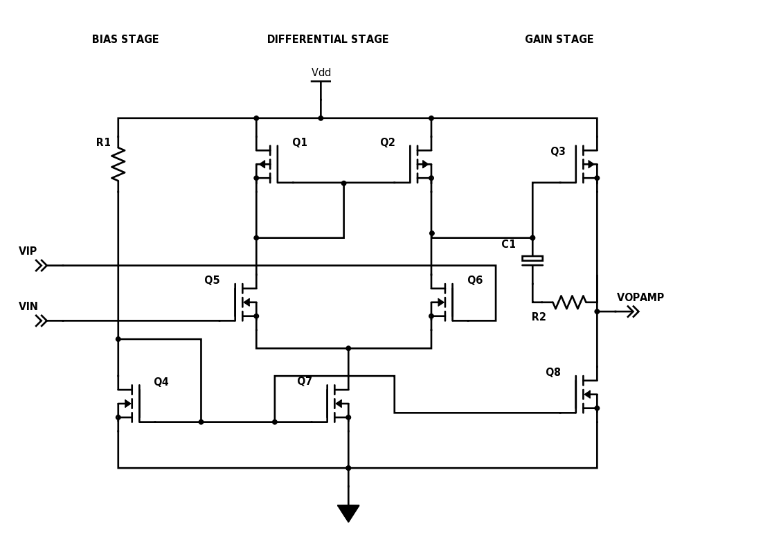
Figure 2: Schematic of two-stage OTA
3. Comparator with hysteresis
Input audio signal is continuously compared with triangular wave to generate pulse-width modulated signal. Hence comparator is a significant block translating input to a PWM wave. This comparator is also designed to have a little hysteresis to avoid false-triggering for a slowly varying input. Hysteresis can be achieved by skewing M3-M6 and M7-M4 mirror pair sizing.
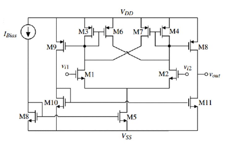
Figure 3: Schematic diagram of the comparator
The output driver consists of two switchs (NMOS and PMOS) that connects the load to VDD (pull-up) or GND (pull-down) and a switch that connects the load to VSS (pull-down). Since on-resistance of the switches has to be made very small to improve power-efficiency, this also run the risk of short-circuiting VDD and GND in the short window of transient edges. The dead-time can be defined as the period during which neither the pull-up nor the pull-down part of the output driver is active. Theoretically, if we had ideal switches, then the dead-time could have been made arbitrarily small. However, given that MOS transistors don't turn off until their VGS drops below VT and that the control signals itself will have a finite slope, we need to introduce some dead time intentionally so as to avoid turning on both pull-up and pull-down networks simultaneously which would effectively short VDD to VSS.
This would result in a large transient current spike since these devices have very high current carrying capacity, and this might destroy the chip. Further, the amount of dead-time introduced needs to be enough so as to be able to avoid shoot-through currents even in the presence of PVT variations. With regards to linearity, dead-time adds non-linearity disturbing linear translation of amplitude to pulse-width. There for there's a trade off between power-efficiency and linearity. C=~2-10pF is a MIM-capacitor that is responsible for providing around 1-15ns non-overlap period.
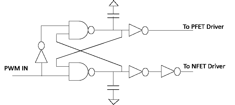
Figure 4: The schematic of the non-overlap generator and the buffers
5. Output driver
Output driver is essentially two switches (PMOS and NMOS) sized wide enough to provide negligeble on-resistance. For an Ron = 0.2 ohms, the width turned out to be NMOS = 1mm/120nm amd PMOS = 3mm/120nm.