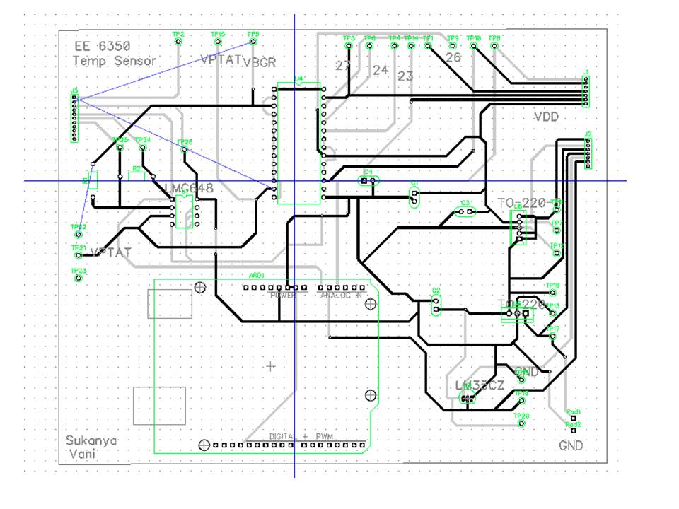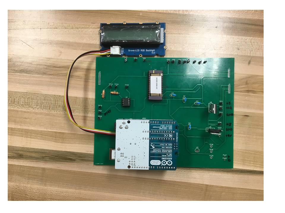
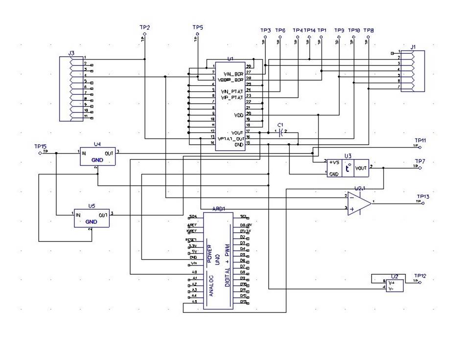
PCB DESIGN
The schematic and layout of PCB is designed using the software DIPTRACE. The chip is placed in the top center and connection for Arduino Uno board is added at the bottom left. The pads for battery of 9V is also provided and an external temperature sensor chip is used in order to compare our chip performance with the former. Two voltage regulators of 1.2 V and 5 V are used to power our chip and external temperature sensor respectively. Various decoupling capacitors are added between the source and the ground. In order to reduce the resistance of routing of wires, they are made thicker.
We have also added an external amplifier so that it can be used if the internal amplifier doesn’t work. Various test pins are connected across PCB for testing purpose. Below are the figures for schematic and layout of PCB.
The PCB Schematic:
The PCB Layout: