LAYOUT
Layout Techniques :
We have used two predominant layout techniques while making the layout of our temperature sensor:
a. Common Centroid
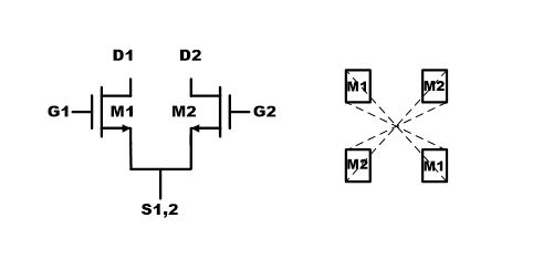
The common centroid technique describes that if there are n blocks which are to be matched then the blocks are arranged symmetrically around the common centre at equal distances from the centre. This technique offers best matching for devices as it helps in avoiding cross-chip gradients as illustrated in the Figure-11 . All the gain devices in amplifiers (error and non-inverting) are laid out as represented in Figure-12 (in the blue box).
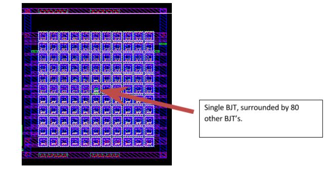
The 80:1 BJT’s in PTAT and BGR circuits are also organized in a centroid fashion as indicated in the figure 13 below:
b. Inter-digitation
Interdigitation reduces the device mismatch as it suffers equally from process variations in X dimension. This technique was used to layout current mirrors and resistors in PTAT and BGR circuits. In the Figure-15 below each brown stick represents a PFET of uniform length. This representation is termed as an inter-digitated layout.
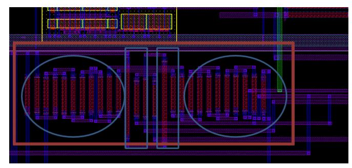
PFET’s (with same W and L) arranged in interdigitated format as shown below in Figure-15 :
c. Dummy Devices:
To ensure better matching of devices (like Resistors, PFET’s and NFET’s) at the end, dummy FET’s or Resistors are placed as the mere ends instead, to minimize the effects of etching during fabrication and thus reduce STI stress. Examples of dummy devices can also be found in the Figure-15 above enclosed in orange boxes.
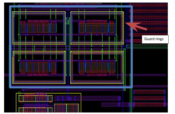
In order to protect high impedance nodes in a circuit from surface leakage, the pads which are used for testing purpose are provided with guard rings.
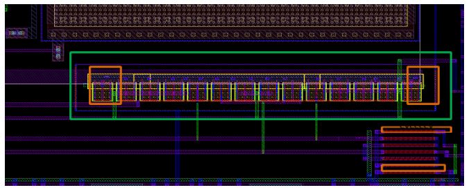
Error Amplifier used in both BGR and PTAT circuits uses both the above techniques and layout is rectangular as shown below in Figure-16:
Layout of our PTAT circuit :
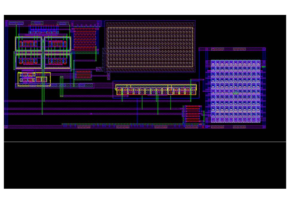
Layout of BGR circuit:
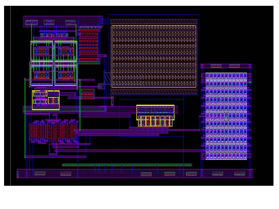
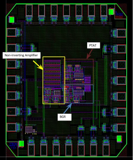
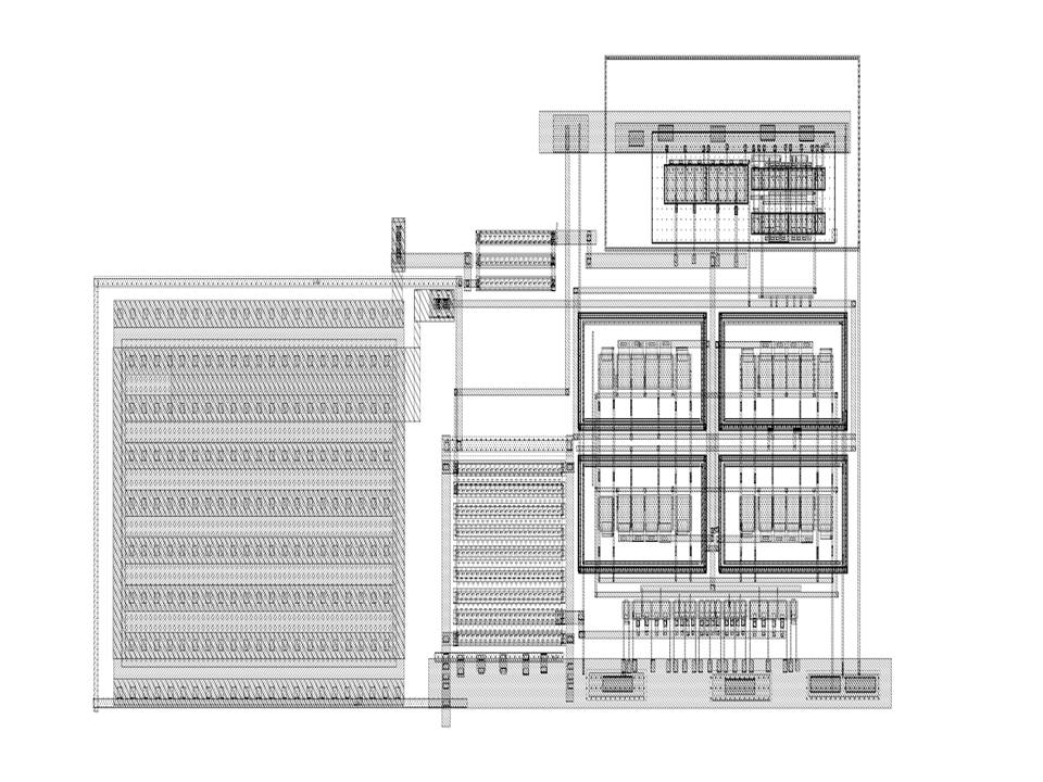
Combining all blocks together with metal filling :