BLOCK DESCRIPTION
System Design:
The entire IC is composed of the following blocks:
a. PTAT circuit
This block is the system block that generates the useful voltage and temperature correlation in the smart sensor.
The circuit can be divided into the following blocks:
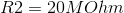
1. Error Amplifier:
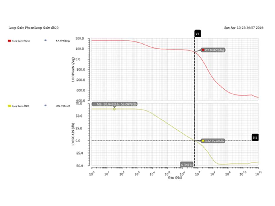
Amplifier Specifications:
| Specification | Target | Simulated |
|---|---|---|
| DC Gain | >60dB | 63.68dB |
| Gain BW | >1MHz | 6MHz |
| Phase Margin | >60 | 67.87 |
| Slew Rate | 10V/us | 6.66V/us |
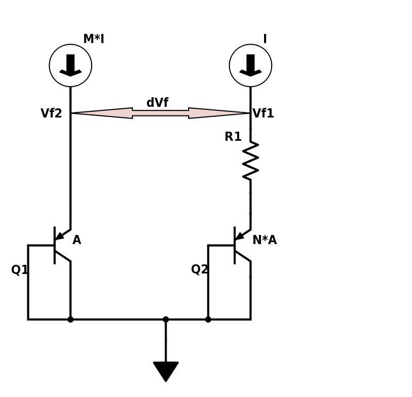
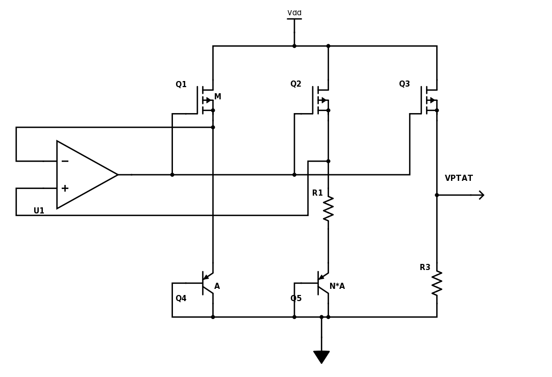
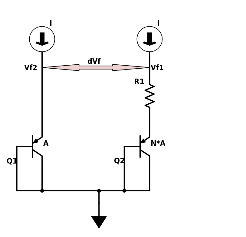
2. Current mirror branches and BJTs
Current Mirror Specifications:

3. Vptat (output voltage) branch
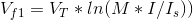
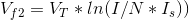
The resistance in the M*I current mirror branch sets up the current in the branch based on Vbe of the two branches. This current will finally be mirrored by the VPTAT branch (The rightmost current mirror branch seen in Figure-7) producing output voltages proportional to absolute temperature.
Since the current in the last two branches are same,

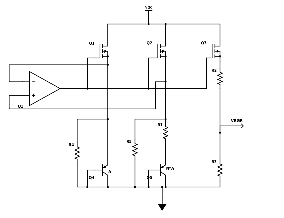
b. Band Gap Reference circuit
This circuit block aims at providing constant bias voltage across all process, voltage and temperature variations. The negative temperature coefficient of base-emitter voltage and positive temperature coefficient of PTAT circuit (∆VBE) are balanced to obtain a BGR voltage with nominally zero temperature coefficient.
The output of this block (Vref) is used as input to negative terminal of non-inverting amplifier for biasing against which a PTAT output (Vptat) is compared to derive a 400mV peak to peak linear output. This linear curve helps in deriving a high precision voltage to temperature correlation.
The circuit can be divided into the following blocks:
1.Error Amplifier
We used the same error amplifier that we used for our PTAT circuit.
2. Current mirror branches and BJTs
Current Mirror Specifications:

3. Vref (output voltage) branch
The resistors in the final current mirror branch in Figure-9 produce a constant output voltage across all PVT corners.
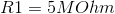
c. Non Inverting Amplifier
This circuit block amplifies the difference between Vptat and Vref. This involves a feedback circuit with resistors of 20M and 5M ohms.
The circuit can be divided into the following blocks:
1. High Gain Amplifier
We reused our error amplifier as the high gain amplifier.
2. Feedback Path:
The feedback path is shown in the Figure - 10 below. The diagram depicts a potential dividing resistor circuit as the feedback network.