
Measurement
DC Operation Points Check
Table 1 shows the value of chip supply and Table 2 indicate the DC operation points of the chip. When testing, to make sure the correctness of each supply, disconnect each supply voltage, current to the pin at first. Test the supply voltage directly and supply current by checking the voltage of relative resistor. Make sure the value of each supply is what wrote in the Table 1. Then connect the supply to chip to test the DC operation points of the chip. Not only to check the correctness of the function of the chip but also to know which corner the chip works under.
By testing the DC operation points, the DC bias condition of the chip is correct and chip works in SS corner. So the generation of the input signal and the anticipation of the output signal should be based on SS corner simulation.
Baseband Test
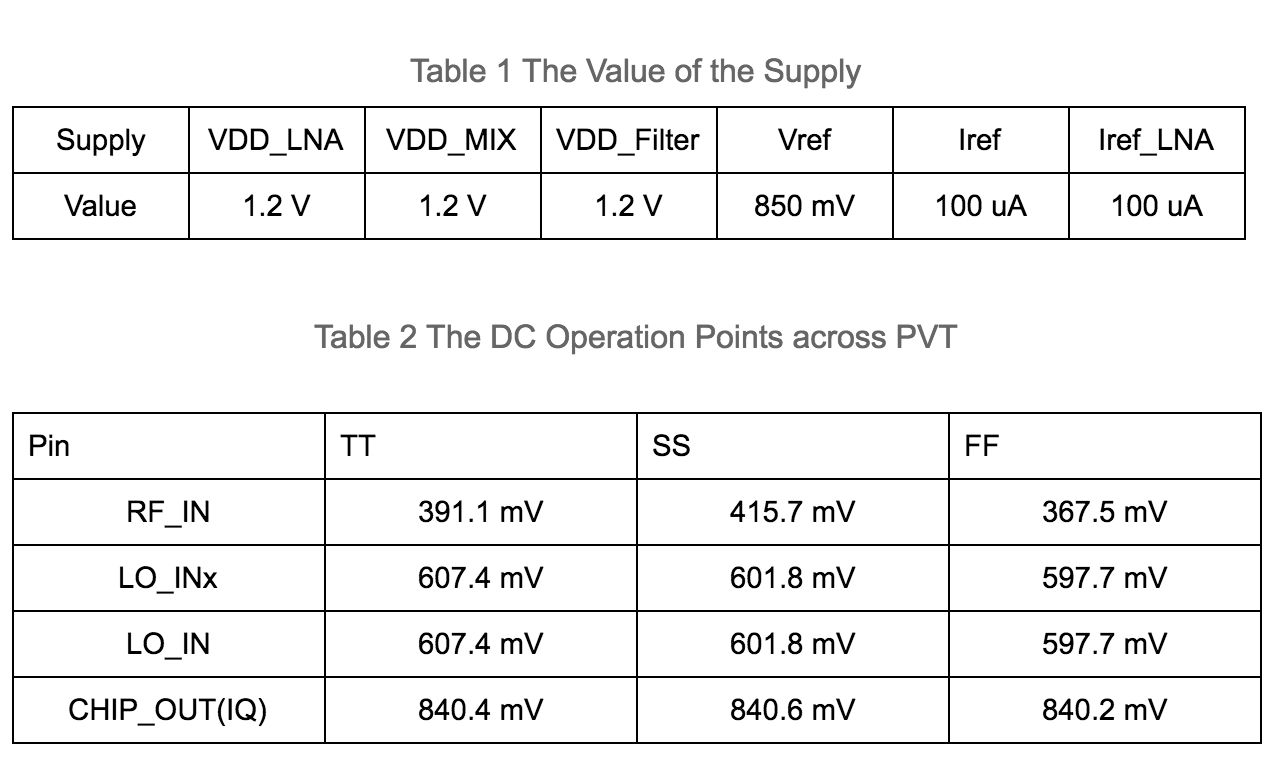
By turning on measurement switch and turning off connection switch on PCB, disconnect RF part with baseband part to test the baseband first. Considering the bandwidth of the filter and the signal we want to receive, use signal generators to generate differential sine waves with 200 kHz frequency. Inject those signals to the input of the filter of the I path and Q path. The chip outputs, which are also the VGA outputs, can be tested by the scope. The waveforms are shown in Fig. 1
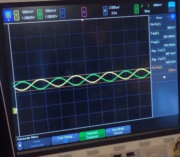
Figure 1 The waveforms of the baseband outputs.
From the Fig. 4.3.1, we can find that the baseband works well. By change the switch control combination, the various gain can be achieved and some waveforms based on different gains are shown below. Detailed measurement and explanation will be discussed in complete chip test.
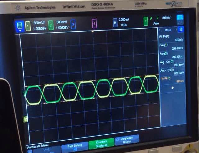
Figure 2 The waveforms of the baseband outputs with different gain
RF Part Test
Still disconnect two part to test RF part. At first, use the to test the S11 of the chip input, which is also the LNA input. From the Fig. 3, S11 is -18 dB at 900 MHz, which is the value as we expected. S11 indicate that the input matching of our design is good.
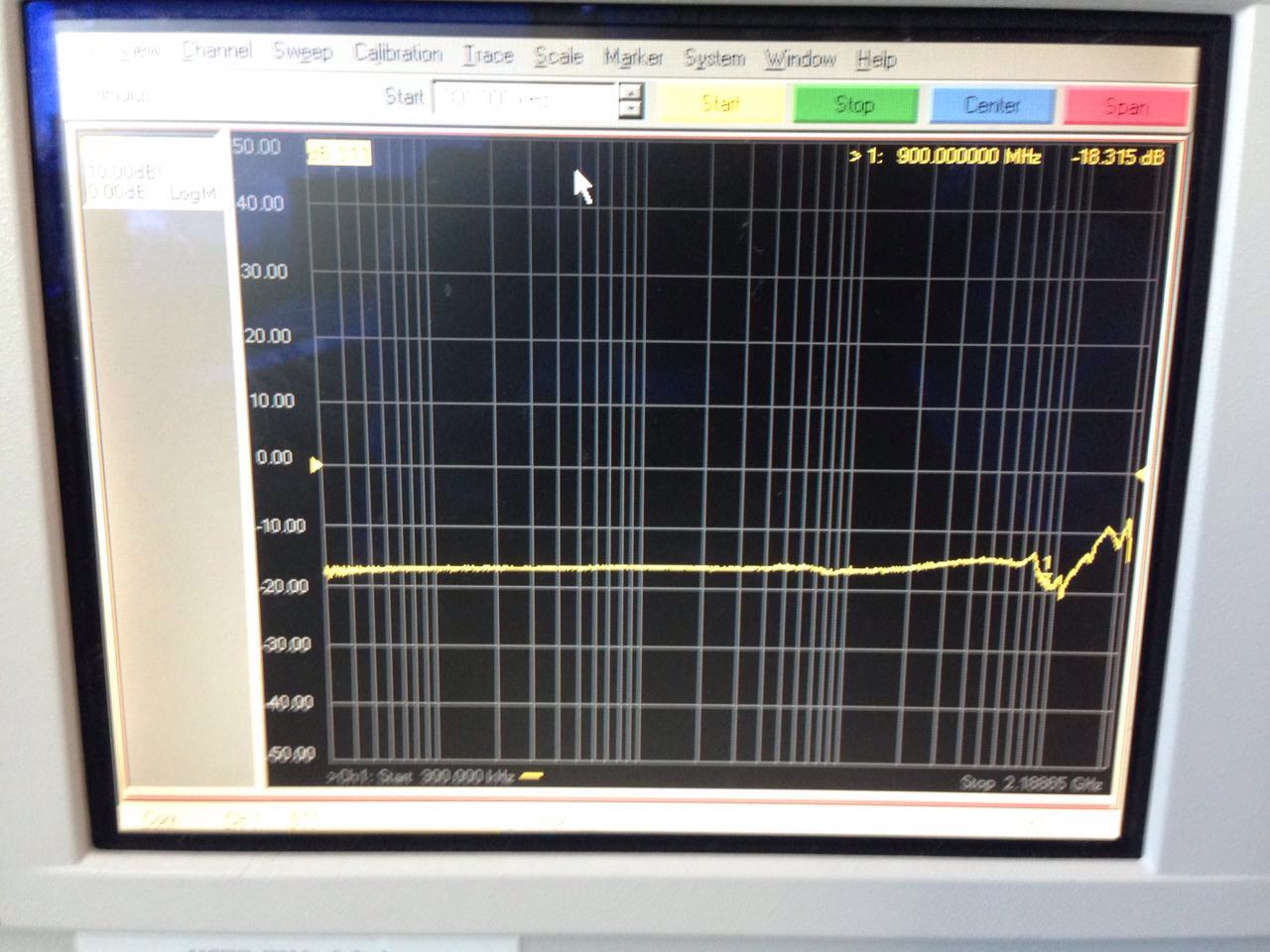
Figure 3 S11 Measurement
Then, inject a 900.2 MHz sine wave as input signal and 1.8 GHz differential sine wave as LO differential inputs. The outputs of the mixer can be tested by scope, which should be two sine waves with 200 kHz frequency and 180 degree phase shift for I or Q path. The scope plot is shown in Fig. 4, from which we can find that the RF part correctly mix the LO clock with input to get the signal we want. Detailed measurement and explanation will be discussed in complete chip test.
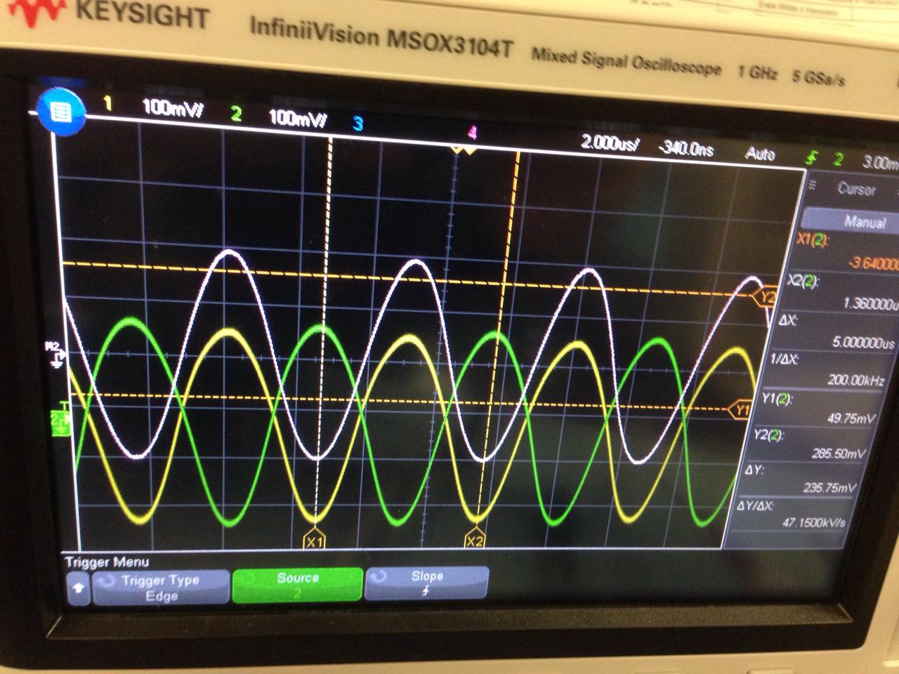
Figure 4 The outputs of the Mixer
Complete Chip Test
From the former test mentioned above, the RF part and the baseband part are proved to work well separately. Now, turn on the connection switch and turn off the measurement to test the function of the complete chip. At first, inject a 900.2 MHz sine wave with -40 dBm amplitude to the input of the chip and differential sine waves at 1.8 GHz with 10 dBm amplitude. All the value of the signal are used based on Cadence simulation when the chip works under SS corner. But no signal can be detected at the chip outputs. By decreasing the frequency of the input signal and LO clock, correct waveforms can be detected on the scope. After several times testing with different frequency below 900M, the reason why the chip doesn't work at 900 MHz is that the amplitude of the LO clock is not large enough. When use LO differential clock with 14 dBm that is much larger than simulation result, waveforms appear at the chip output. The transmission lines of the LO differential inputs on PCB may not designed well so that much loss is generated. Also, the IQ generator may not designed and layout well to generate more loss than expected. Finally, when appropriate input signal and LO clock are given, the correct waveforms can be detected by scope. Fig. 5 shows the I path differential outputs of the chip, when VGA provides 0 dB gain. From the figure, differential outputs are both sine wave with 200 KHz frequency, which is exact signal frequency we want to receive. Also, 180 degree phase shift between outputs is what we expected.
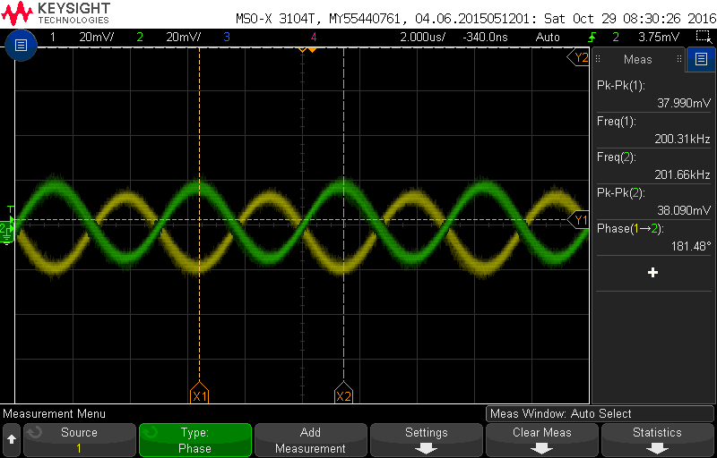
Figure 5 I path chip outputs with 0 dB VGA gain
Fig. 6 and Fig. 7 shows the I path differential outputs of the chip, when VGA provides 0 dB, 15 dB, 19 dB, and 40 dB gain. So, 0 to 40 dB gain are proved to be available by the chip. When calculating the amplitude ratio of different gain waveform to the 0 dB gain one, exact gain can be got as the simulation results. Because when the gain of the VGA is 40 dB, the swing of the outputs is out of the range so the waveforms have flat peak value.
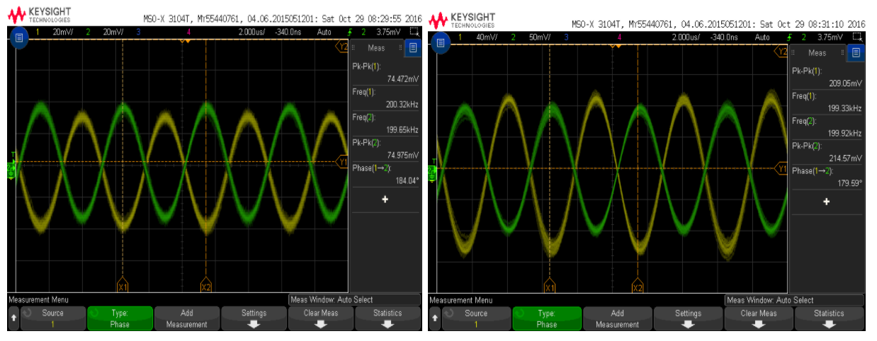
Figure 6 I path chip outputs with 6 dB and 15 dB VGA gain
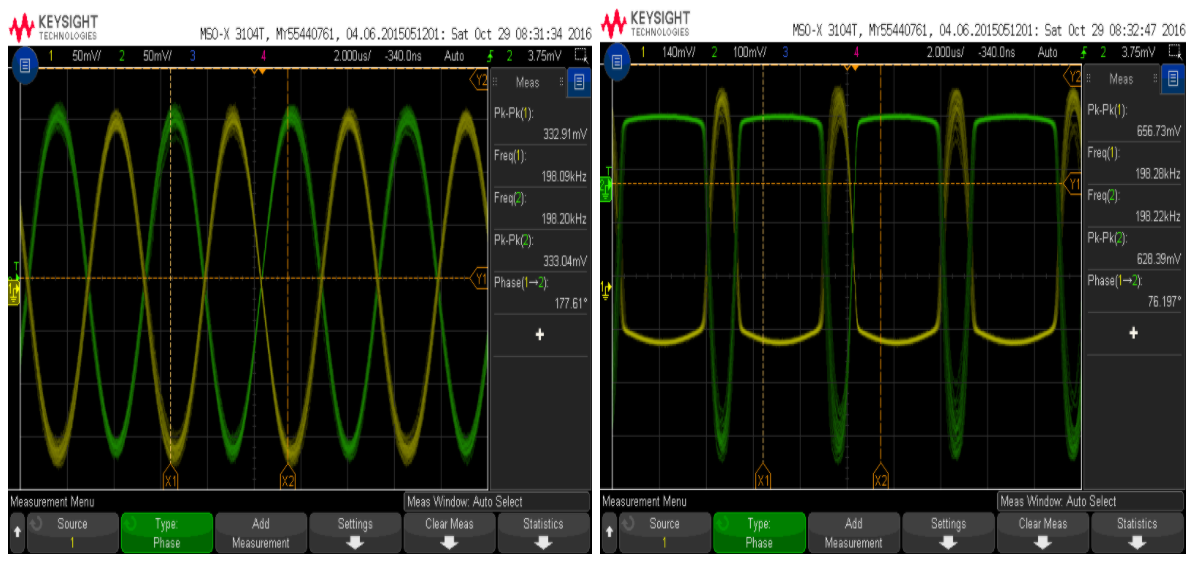
Figure 7 I path chip outputs with 19 dB and 40 dB VGA gain
The positive outputs of both I and Q paths are shown in Fig. 4.3.9, in which the yellow wave is from Q path and the green wave is from I path. The amplitude of the waveforms of the two paths are not the same. Also, the phase shift between I and Q paths is just 83 degree, which is not equal to 90 degree as we expected. By several testing, the main reason we think is that the outputs pins of the I and Q paths are all at the top of the chip. But actually, the outputs of the baseband parts used in the I and Q paths are near the right side of the chip. So during the whole chip layout, we need to route the baseband outputs to the chip output pins. Definitely, the length of the routing lines for I path and Q path are different, which generate mismatch between the outputs of the I and Q paths.
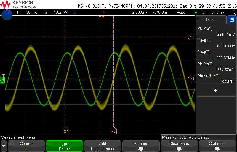
Figure 8 The positive outputs of both I and Q paths