
Circuits Design
Low Noise Amplifier
This the project "RF Front-End Receiver for ISM-900M" webpage. It is the part of the course " VLSI Design Lab (E6350)",taught by Prof. Peter Kinget in Spring 2016 at Columbia University. Thanks MOSIS for kindly offering the opportunity to fabricate this chip
The following section describes the trade-off and key design concepts for the LNA. As the first step, the specifications of the LNA on a system level have to be determined. The LNA has two main functions: it needs to amplify the signal with a high gain in order to reduce the effect of the noise of consecutive stages, and it also needs to achieve this goal while keeping its own noise figure as low as possible. Keeping the noise figure below 3dB and the voltage gain higher than 15dB are the goals for the initial design. Finally, a good input matching is required. A -15dB reflection coefficient is the value used in most applications as well as in this design. One characteristic, which was very important for the choice of the LNA topology, is that it has to go from a single-ended input to a differential output. The topology chose for this design is a common- source, common-gate noise-canceling structure as shown in Fig. 1. Other than the advantage of noise canceling, it is a wideband LNA, and thus for the purpose of input matching, it does not need separate matching circuits for the 950 MHz and the 1850 MHz operating point.
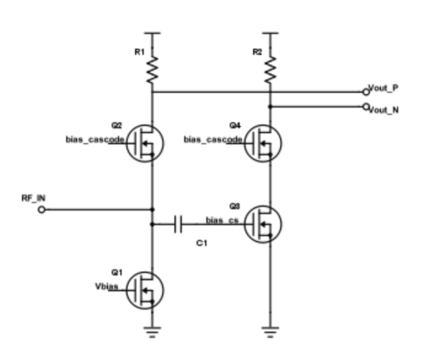
Figure 1 Simplified Schematic for LNA
Double-Balanced Mixer
The mixer needs to convert the RF signal to a much lower intermediate frequency with a large conversion gain to meet the overall specification of 40 dB conversion gain. Since the mixer comes after the LNA, a good linearity would also be required. In order to achieve a low 1/f corner frequency, keeping the flicker noise in this block low is also an important requirement. For the mixer, a double balanced topology, as shown in Fig. 2, was chosen. Comparing to the passive mixer, the active typology could provide more gain and better switching (by biasing the switching transistors at the pivot point right between the triode region and the saturation region and driving it with a sine wave). The double balanced mixer was chosen because it could improve the linearity and suppress both the RF feedthrough and LO feedthrough. Both the RF feedthrough and the LO feedthrough are canceled out by the double balanced structure. Also, we eliminated the current source at the bottom of the mixer to provide more headroom for our design.
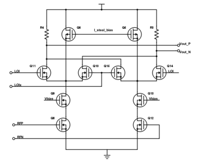
Figure 2 Simplified Schematic for Mixer
I/Q Generator
The I/Q generator needs to take a 300 mV sinusoidal input signal, buffer it, and then generate four output waves, which are 90 degrees out of phase and have a rise and fall time around 50 ps. We split up the LO buffer and I/Q generation in three stages, as shown in Fig. 3. The first buffer, which consist of two inverters, is used to buffer the off-chip LO sinusoidal voltage source. The first inverter has a resistor feedback to set the DC voltage, and the second inverter is added to increase the driving power.
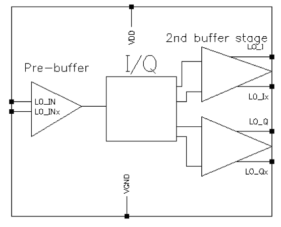
Figure 3 I/Q Generator Block Diagram
The second block is the I/Q generator implemented using two latches connected in negative feedback [2]. The connection of the two latches is shown in Fig. 4 (a). These two latches (Fig. 4(b)) form a divide by two circuit, and this means that the frequency of the LO has to be twice as high as the expected output frequency. The I/Q generator produces four outputs, which are 90 degrees out of phase.The last block is an extra inverter to increase the slew rate. It consists of three stages, which were designed to increase the load capacitance with a factor of four in every stage as is done in most digital circuits. It is not perfectly a factor of four since it was also important to keep the duty cycle as close to 50 percent as possible. The duty cycle will change a little when the frequency changes, so it was attempted to keep the offset as small as possible for both cases.
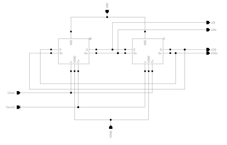
Figure 4(a) Divide-by-two circuit
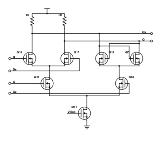
Figure 4(b) Simplified Schematic for the latch
Filter
To determine the parameters of filter, the output signal of the mixer should be considered. Based on the simulation for the output signal of the mixer, the flicker noise is comparatively large under 100 kHz. So it is better to arrange signal around 200 kHz. The further down-convert process can be down out of chip to receive the audio signal. Due to output signal figure and considering PVT toleration, the bandwidth of the filter is set to be 250 kHz. To get a sharp slope in transition band of the filter, Tow-Thomas Biquad structure is employed, as shown in Fig. 5. The transfer function of this structure is formula (1) shown below . So we can derive that w0 = 1/(RA*CA) is equal to and Q = CA/CB. To make the DC gain of filter become 0 dB, -k0 = 1/(RB*RA*CA^2) should be equal to 1. In order to get flat frequency response, Q should be equal to 0.707. In the schematic design, RA and RB should be large enough, which means the resistance at OPAMP output node is large so that the large open loop gain can be guaranteed. But considering layout and chip size, the large value of resistance means a large area, which should be compromised. In addition, desired value of resistance and capacitance may not be achieved when we use real chip passive component. Finally, RA = RB = 2.46.731 k, CA = 2.5 pF and CB = 3.5 pF are used in the schematic, which can achieve 0= 258 kHz and Q = 0.714.
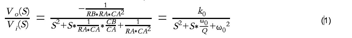
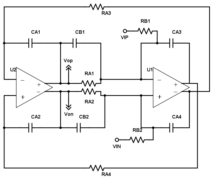
Figure 5 Biquad filter structure
VGA
In this design, we suppose that the minimum input signal is -80 dB. Because LNA and Mixer have totally 40 dB gain, to set the output signal at 0 dB, the VGA should have 40 dB maximum gain. In addition, the VGA output is also the output of the chip. To receive an audio signal and do further signal process after receiver output, we set the output swing of VGA be 400 mVp. If just use one stage feedback network, the closed-loop gain 1/belta = 100. To meet A*belta >> 1, A should at least be 1000 to make sure the gain error. It's hard for us to design an OPAMP with such big gain and output swing with a supply voltage ( Vdd ) is just 1.2 V. So we decide to implement two stage cascade with each stage providing maximum gain 10 so that OPAMP just need gain above 100 V/V. The VGA structure is shown in Fig. 6.
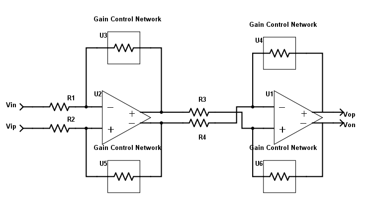
Figure 6 The VGA structure
Furthermore, design cycle is very tense for us so that we don't want to make the whole circuits too complex. Then just use 4 parallel resistors with pmos switch to realize the gain control network. The control network structure is shown in Fig. 7.
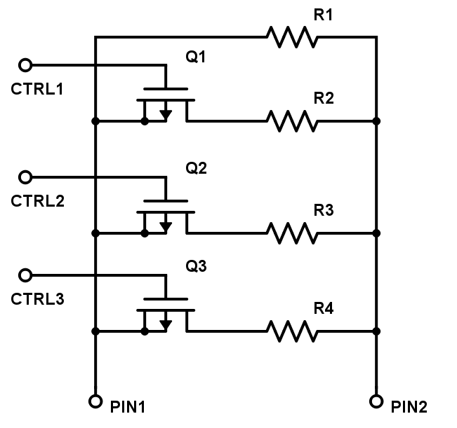
Figure 7 Feedback network
OPAMP
The fundamental of VGA and filter is OPAMP. To simplify our design, we want to use the same OPAMP for both VGA and filter. Because the requirement of OPAMP in the filter is far easier than in VGA, many parameters of OPAMP is determined by VGA requirement. As mentioned above, to ensure A*belta >> 1, A should be larger than 100, which is equal to 40 dB. Considering PVT and load due to feedback network, set OPAMP gain = 50 dB to provide the margin for design. In addition, the chip output swing should be 400 mVp, which are also the outputs of the OPAMP used in VGA. So OPAMP should provide enough output swing. Because the phase margin of filter and VGA are smaller than OPAMP, to achieve 60 degrees phase margin of those two, set the phase margin of the OPAMP to be 85 degrees. Finally, the dc voltage of output of the mixer, which is input of the filter, is very sensitive. From our design and simulation, the outputs of the mixer have 850 mV dc value. So the OPAMP should be able to process signal with that dc value. Actually, the connection between filter and VGA is also the connection between one OPAMP and the other. So it's convenient to set the output common-mode voltage of the OPAMP to be equal to its input common-mode voltage, which can be realized by common-mode feedback.
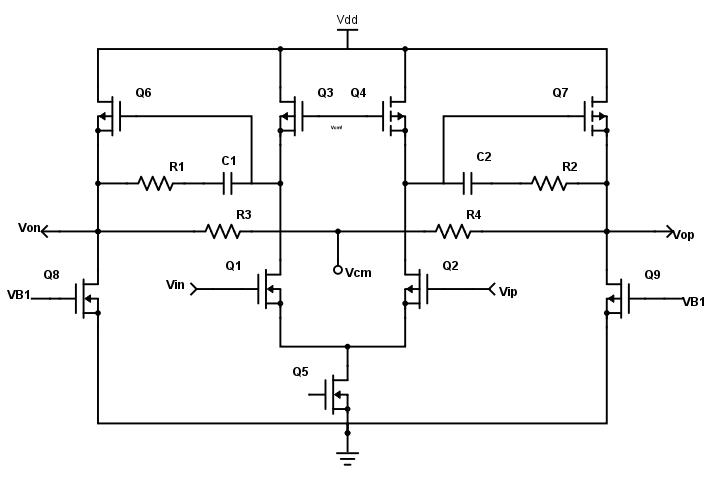
Figure 7 Two stage OPAMP structure
As mentioned above, the output common-mode voltage should be 850 mV and output swing should be 400 mV. With supply voltage being just 1.2 V, the two stage must be chosen. Also, to ensure the second stage amplifying transistor in saturation, the pmos is chosen to be the input transistor of the second stage. Because just 50 dB is needed, the simple two stage is enough for OPAMP. The structure of two stage OPAMP is shown in Fig. 7. The resistors R3 and R4 in Fig. 7 are used to detect the common-mode voltage of the differential outputs of the OPAMP. Then send it to common-mode feedback circuit to generate feedback voltage by compared with reference voltage Vref. The common-mode feedback circuit is shown in Fig. 8. The value of compensation capacitances c1 and c2 can be determined by wt=gm1/C. The value of compensation resistors R1 and R2 can be determined by phase margin, which has equation P.M.=90°-arctan(ft/fp2)-arctan(ft/fz).
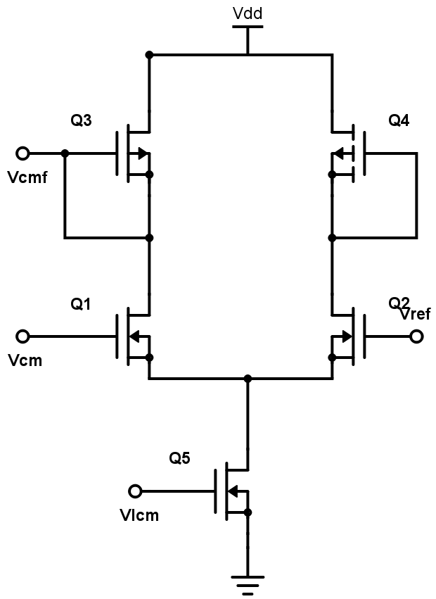
Figure 8 Common-mode feedback circuit