
Test Plan and PCB Design
Test Plan
When a chip is fabricated and sent back, testing and the measurement should be taken to verify the function of the chip. So test plan is needed. There are several test steps should be performed for verification.
(1)The customized PCB should be designed to accommodate the chip. Also, the design of the PCB should leave enough margin to make sure the realizability in the various scenario.
(2)Measure and adjust various suppliers to provide correct voltage and currents. In addition, check the DC operating points of the chip to know whether it works well or not and the corner of the chip.
(3)Measure the S11 of the input signal of the chip to observe the performance of the LNA design.
(4)Test the RF part ( LAN, Mixer, IQ ) and the baseband part ( Filter and VGA ) separately, by making the connection switch off and the measurement switch on to disconnect two part. Inject 900.2 MHz input signal and 1.8 GHz LO clock, so we can test the RF part by measuring the waveforms at the outputs of the mixers on the scope. Provide 200 kHz differential signal at the inputs of the filter, so baseband part can be checked by measuring the waveforms at the outputs of the chip on the scope.
(5)Make the connection switch on and the measurement switch off to connect RF and baseband part. Also, inject 900.2 MHz input signal and 1.8 GHz LO clock, but measure the outputs of the chip on the scope to test the whole chip performance.
PCB Design
To test the chip, a good customized PCB is very important and fundamental. According to reality and the design scale, the two-layer board is used. Because of the pad position and size of the QFN 28 package, we can't test the chip on the bread board in advance. So when designing the PCB, enough margin should be left to accommodate to the different scenario. For each power supply pin of the chip, a jumper and a header are used to connect with the voltage regulator to make sure the chip not broken. Supply current is generated by including a series potentiometer, which can be tested by test points parallel to the potentiometer. For LNA, we design two paths for the input signal. One is directly connected to SMA, which is used when the input signal is generated by the signal generator. Another is connected to SMA with resistors attenuation network, which is used when the input signal is generated by some other evaluation board. For LO, differential inputs are connected to two SMA. The coplanar transmission lines are employed for both LNA and LO inputs. The width of the line is calculated by ADS to get 50 Ohm.
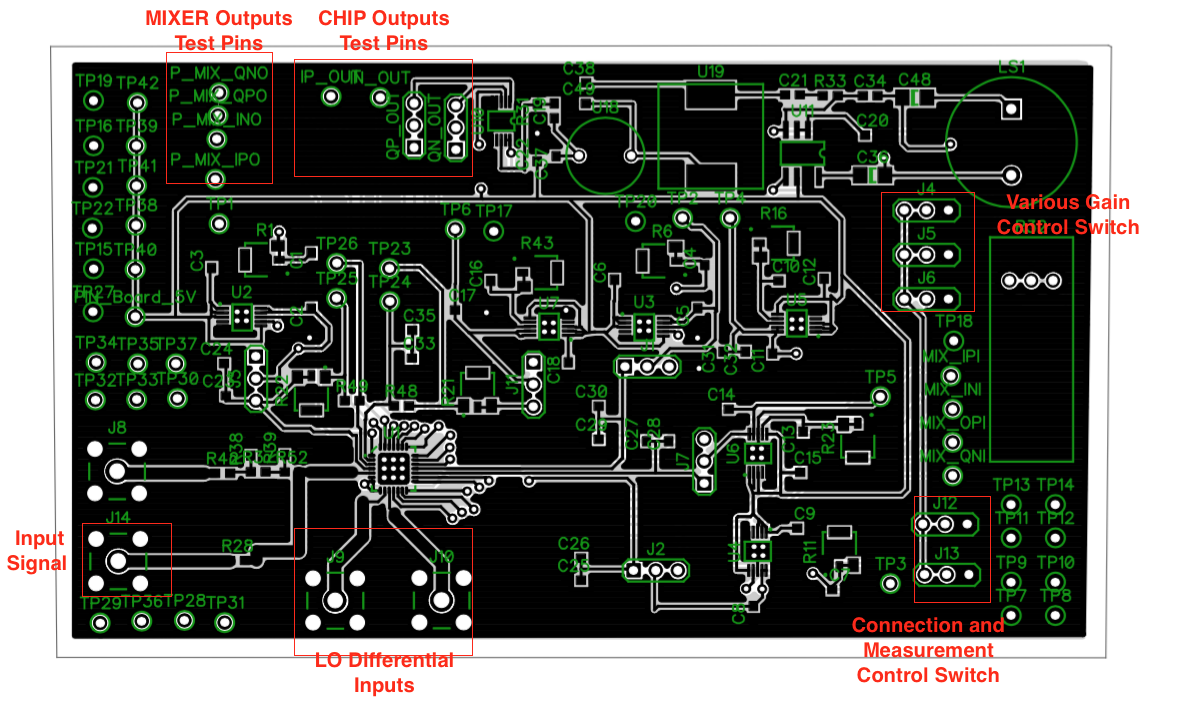
Figure 1 The design of the PCB.
The design figure of PCB and the PCB after soldering are shown in Fig. 1 and Fig. 2. When designing the PCB, because we consider the various testing situation ( Due to lab condition, some equipment may not be used ), we usually design two plans for each point we want to test. So, some components and test points are left blank when soldering.
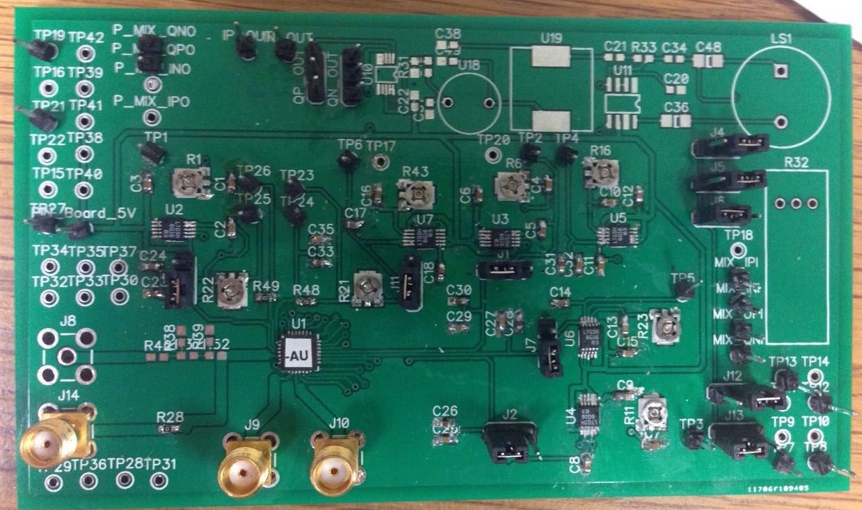
Figure 2 PCB after soldering