
Physical Design
The layout of the chip is shown in Fig. 1, corresponding to QFN 28 package
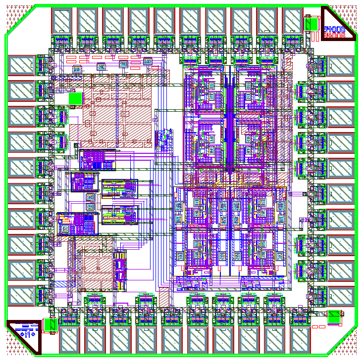
Figure 1 The layout of the chip
LNA
Since LNA is the first block of the receiver chain, extra cares are needed during the layout to make sure the RF signal get amplified properly by the LNA with enough gain and minimal noises. As shown in Fig. 2, the RF components are placed as close as possible to minimize the effects of the parasitics. In order to make the resistor value more accurate and robust to process variations, multiple resistors are connected in parallel to achieve the desired value. RF transistors are used in the LNA to provide an more efficient layout with better parasitic modeling. Moreover, guard rings are added to minimize the substrate noise coupling, and decoupling capacitor were added at the right hand side for each DC point.
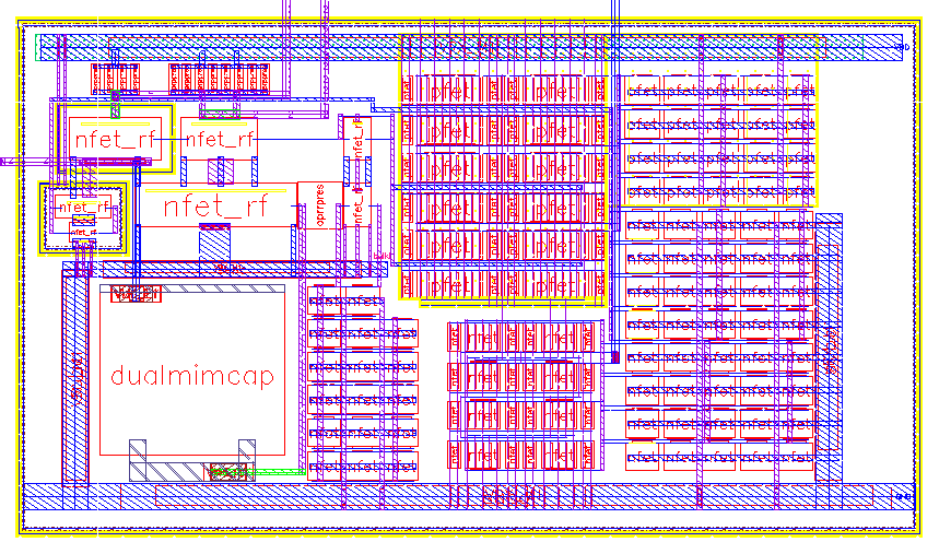
Figure 2 The layout of the LNA
IQ Generator
Because the IQ generator is very sensitive to mismatch. When lay the IQ generator, we really care about the symmetry and make sure that each signal path has the same distance or length of the connection line. The layout of the IQ generator is shown in Fig. 2.
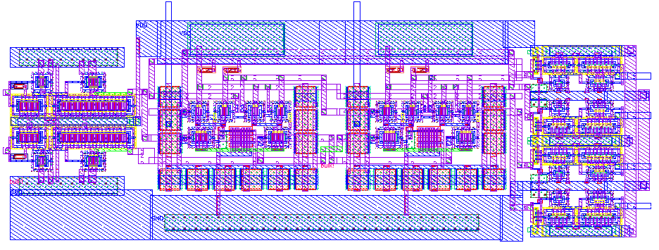
Figure 2 The layout of the IQ generator
Double-Balanced Mixer
Fig. 3 shows the layout of the double balanced mixer. In order to minimize the coupling between the LO signal and the RF signal, these two signals are routed orthogonal to each other with shields added between them. Since the mixer is differential-in differential-out, matching is also critical to the this layout. As you can see from Fig. 3, transistors are placed as close as possible to minimize the parasitics. Positive and negative path are symmetrical to each other, and signal routings are also match
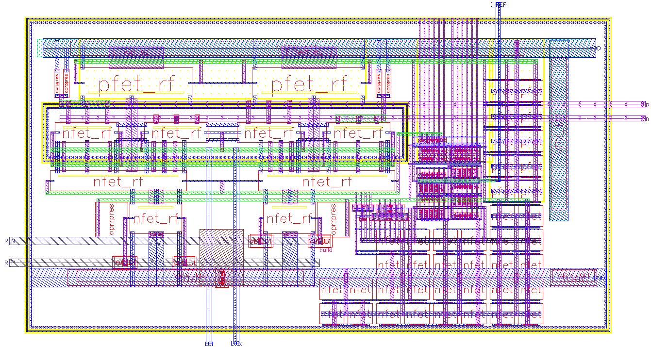
Figure 3 The layout of the Mixer
OPAMP
During layout, parasitic effects and mismatch must be careful of. Because of differential design, ensuring the symmetry of the circuit is a way to decrease mismatch. Using multiple fingers to make the width single finger and length of each device be the same can also reduce the mismatch. To decrease gate resistance, multiple fingers is useful and have their gate fingers connected using M1 to reduce ohmic resistance instead of using poly-silicon. The layout of OPAMP is shown in Fig. 4
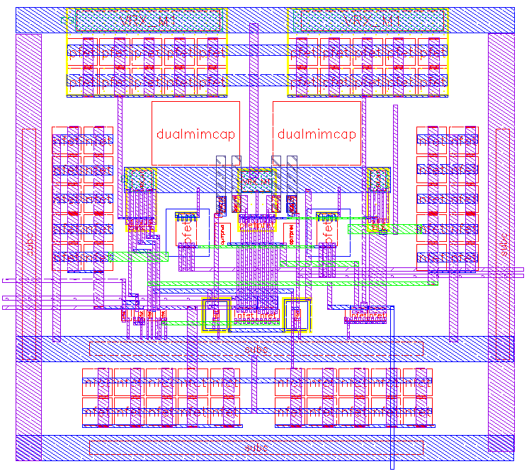
Figure 4 The layout of the OPAMP
Filter
The layout of the filter is shown in Fig. 5. The basic cells are two OPAMPs mentioned above. Also, in the layout, the whole system construction should be considered, including the connection between the filter and the mixer at the input, the VGA at the output. Guard rings are employed to minimize the substrate coupling.
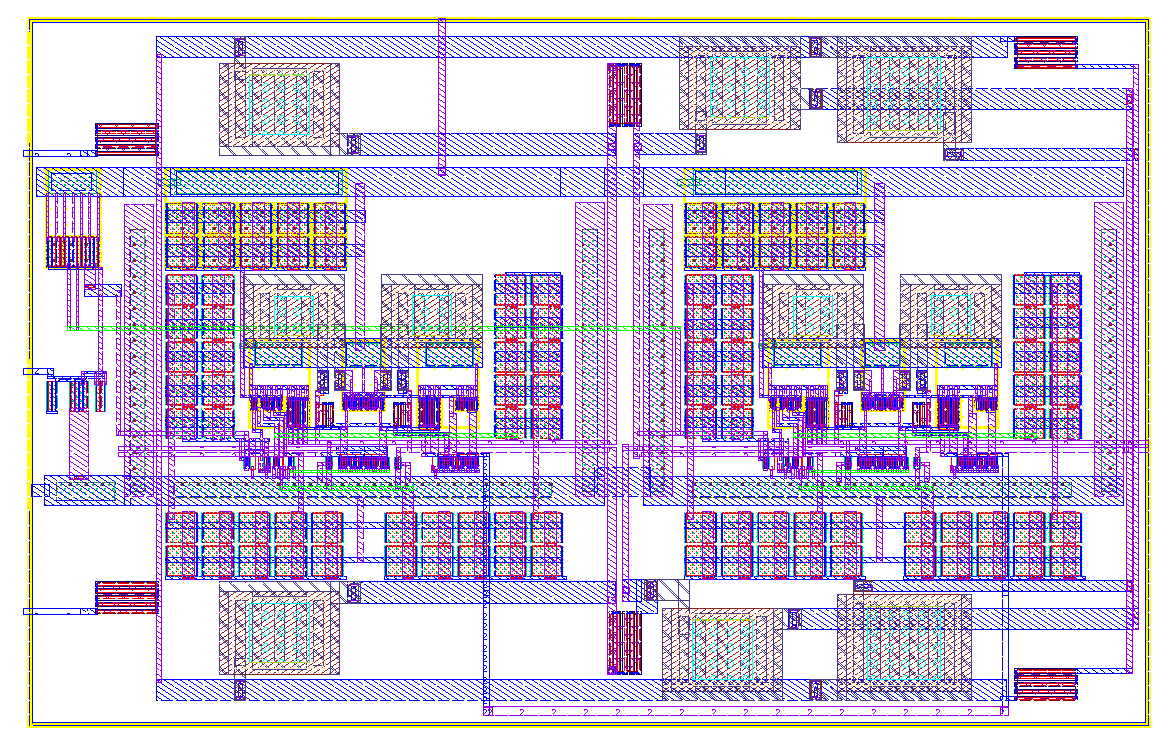
Figure 5 The layout of the filter
VGA
The layout of the VGA is shown in Fig. 6. The basic cells are two OPAMPs and two gain control networks. Also, the guard rings are employed to minimize the substrate coupling.
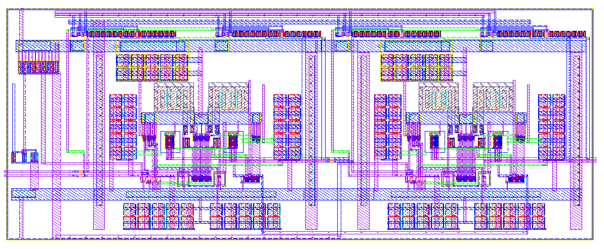
Figure 6 The layout of the VGA