
Testing
A PCB test platform was designed and fabricated to test this chip. Single-ended test input singals were converted to differential via input transformers. The differential input common-mode voltage was set by the VBIAS output of the chip connected to the center tap of the transfomer. The differential chip "current" outputs were converted to the voltage domain via transimpedance amplifiers. They also provide amplification to enhance noise measurements. The diffenential TIA outputs are converted to single-end signals via transformers. THe chip and PCB support a signal path identical to the filter signal path, except the filtering function. Effectively subtracting the effects of this path through calibration and measuremnts, enables measurements of only the filter circuits. The PCB includes linear voltage regulators to provide "clean: power for the 1.8V, +5V, and -5V domains. The 1.8V domain (chip VDD) can be adjusted for +/-10%. A VBIAS buffer circuit is included but not used.
An Arduino GPIO board was used to drive the serial interface signals to control the cut-off frequency trim. The Arduino board support package was used in MATLAB along with a MATLAB script to poke the signals.
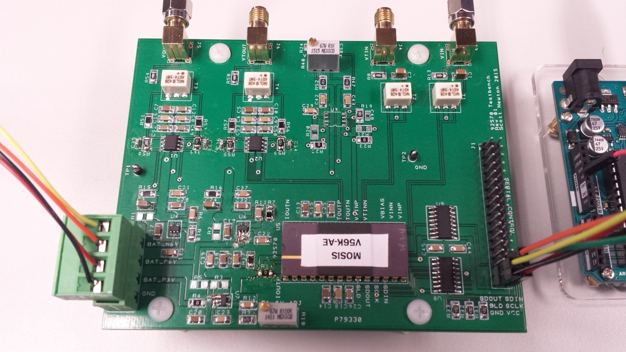
Figure 10. PCB Assembly with Arduino Attached
The filter design was fabricated in a 0.18um CMOS technology. Fig. 11 shows the die photograph; the active area of the filter is 0.33mm2. Fig. 10 shows the measured filter response for all 11 trim settings. The nominal trim setting yields a 3dB-cutoff frequency of 13MHz. The trim range is 10.2MHz to 18.1MHz. Performance metrics from simulations and measurements are compared in Table I. The PEX (including R and C parasitics) simulation results are almost identical to the schematic simulation results. Performance was measured on a manufactured chip installed in a discrete circuit test platform. The measured performance validates the simulation results.
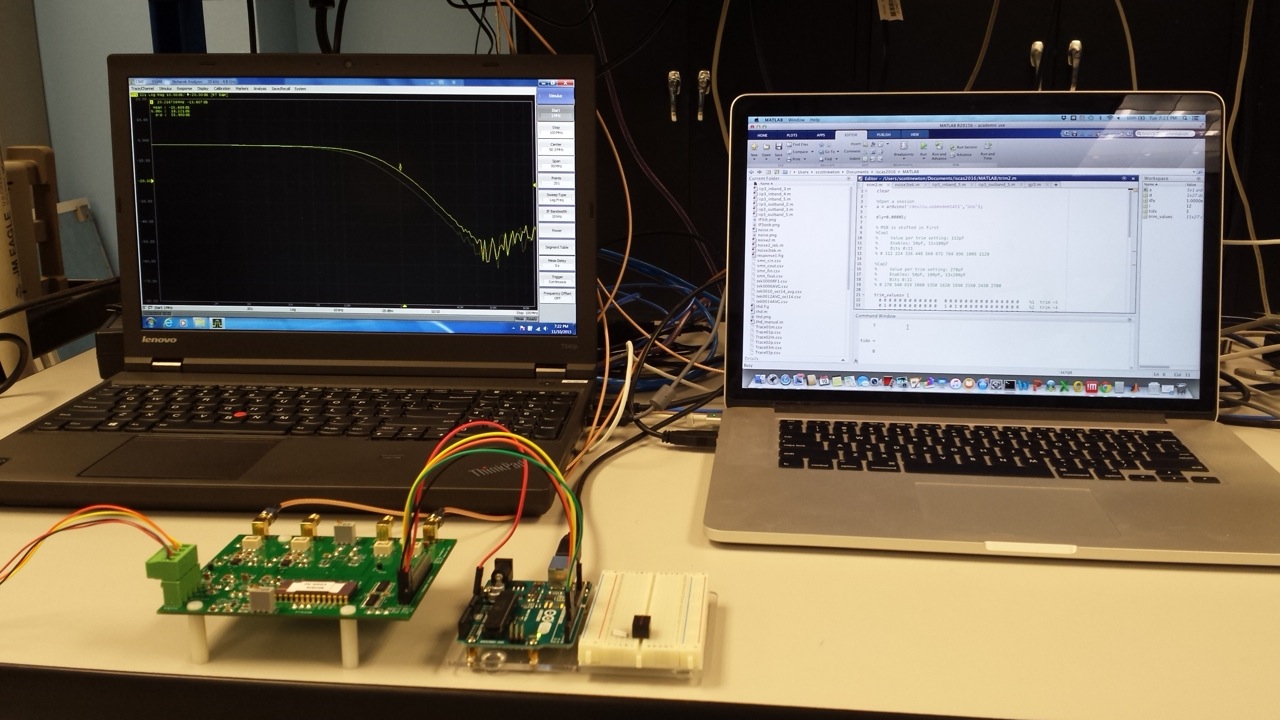
Figure 11. Lab Set Up for Lab Measurements
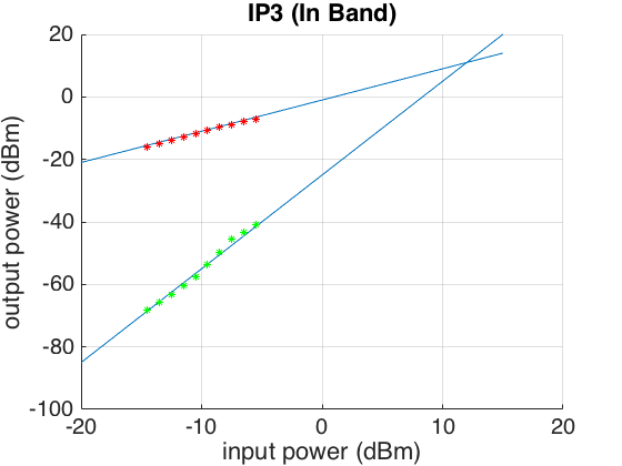
Figure 12. In-Band IIP3 Lab Measurements Plotted in MATLAB
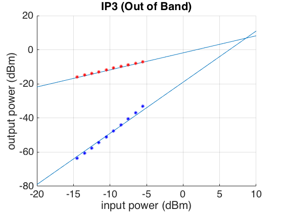
Figure 13. Out-of-Band IIP3 Lab Measurements Plotted in MATLAB
Table I. Lab Measurements and Simulation Results
| Metric | Simulation (Schematic) | Simulation (PEX) | Measurement (Chip) |
| Supply Voltage | 1.8V | 1.8V | 1.8V |
| Supply Power | 16.6mW | 17.7mW | 15.5mW |
| fcutoff (-3dB) | 16.1MHz | 13.3MHz | 13.0 MHz |
| Trim Range | 13.1-19.8MHz | 11.1-17.5MHz | 10.2-18.1MHz |
| In-Band IIP3 (@6MHz, 8MHz) | +0.90dBV | +0.89dBV | +0.89dBV |
| Out-of-Band IIP3 (@30MHz, 50MHz) | -9.6dBV | -9.1dBV | -4.4dBV |
| Input 1% THD @1MHz | 0.18Vrms | 0.19Vrms | 0.15Vrms |
| Input 1% THD @10MHz | 0.30Vrms | 0.35Vrms | 0.27Vrms |
| Input Referred Noise* | 150uVrms | 171uVrms | 166uVrms |
| Dynamic Range** | 67dB | 66dB | 64dB |
* Integrated over 1kHz-20MHz
** Ratio of 1% THD @ 10MHz to Noise floor
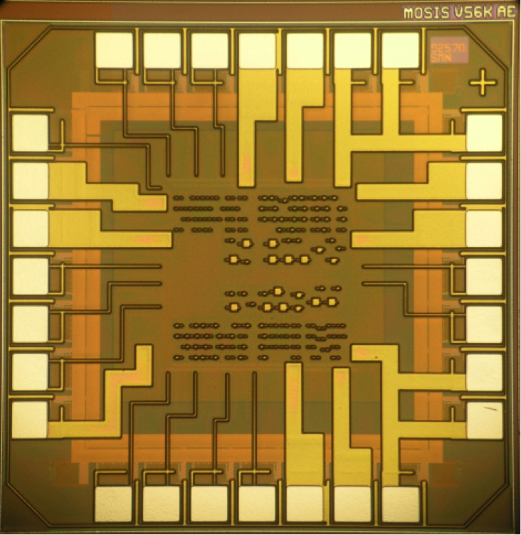
Figure 14. Die Photo
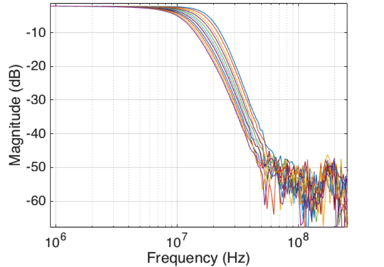
Figure 15. Filter Frequeny Response