
Die Design
Standard-Cell-Based Analog Design & Layout Flow
A traditional analog chip design flow is compared to the standard-cell design flow in Fig. 4. The Design Schematic development time can benefit a reduction thanks to using a pre-defined set of library primitives. The digital design community has long recognized that writing HDL code can be more efficient than drawing a schematic. Furthermore, design reuse tends to be easier for the text-based HDL code. However, the key advantage of the standard-cell flow is the dramatically faster physical design. Since place and route is automated, very fast layout generation can be accomplished. For the presented filter design, constraining the design for placement with die planning, power planning and floorplanning took less than an hour and APR took less than a minute! (vs. an estimate of days in manual design flow). This enables rapid design iterations with parasitic extraction from DRC-correct layouts at a fraction of the time required for traditional manual design iterations.
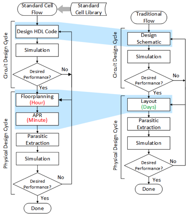
Fig. 4. Traditional Analog Design Flow (right) and the proposed standard-cell based analog flow based on a digital logic Place-and-Route flow using standard cells (left); Actual (red) and estimated (green) time periods for this filter design.
Adding Custom Cells to the Standard Cell Library
A standard cell library enables automated layout in the digital chip design flow. Typically these cells are digital functions such as logic gates, flip-flops, counters, etc. Each cell adheres to predefined geometries enabling auto-placement and auto-routing. A unit standard cell typically has PMOS and NMOS regions arranged as “stripes” as shown in Fig. 5(a). PMOS towards the top with power supply rail trace and NMOS towards the bottom with ground (GND) trace. Signal traces must fall on grid intersections to enable APR connections. The high level standard cell library design flow is shown in Fig. 6. For tall cells, the height must be extended by multiples of a single cell height to avoid shorts with regularly spaced power and GND rails (see Fig 5(b)). A cell can be any multiple width of λ. An abstract view containing only metal layers, used by APR to avoid shorts and make connections, must be added to the library after the cell design is complete.
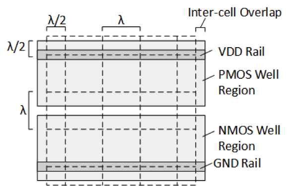
Fig. 5(a). Structure of a single-height standard-cell layout template
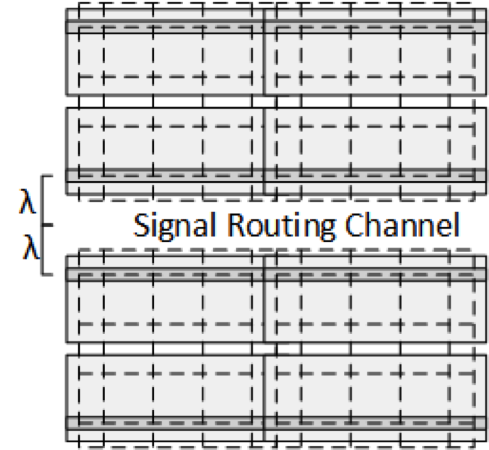
Fig. 5(b). Structure of a multi-height standard cell layout template

Fig. 6. Standard Cell Development Flow
An existing digital logic standard cell library was used as a basis to create the filter’s custom analog standard cells consisting of two inverters, a transmission gate and capacitors. To extend the sizing range available to the analog designer, the required two new inverters were designed by modifying an existing basic inverter cell. Similarly, a transmission gate cell was added starting from the basic inverter cell (see Fig 7(a)). A set of four standard cell capacitors with values of 50fF, 100fF, 500fF and 1pF (see Fig. 7(b)) was created and through parallel combinations, other values can be made in HDL code.

Fig. 7(a). Analog Standard Cell Layout Examples: Transmission Gate

Fig. 7(b). Analog Standard Cell Layout Examples: 1 pF Capacitor
Verilog HDL Design Capture
The entire filter design was captured in Verilog HDL as a netlist of interconnected standard cells. The digital logic and clock tree could have been synthesized, but since the register pipeline architecture ensures adequate setup and hold times, logic synthesis was not included to simplify the tool flow. Fig. 8 shows example Verilog code specifying the inverter-based transconductor. To simplify floorplanning, the HDL design hierarchy was carefully planned so that related circuitry, to be placed together, is included in the same sub-function.
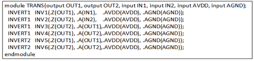
Fig. 8. Transconductor Structural HDL Code (Verilog)
Simulation Verification
Simulations were run in the circuit design phase using the schematic auto-generated from the HDL netlist. Design iterations over component values and cell sizes continued until satisfactory performance was achieved. After the physical design phase, the same simulations were run with R and C parasitics extracted from a layout (PEX). For this design, only one iteration was required since satisfactory performance was achieved with the first layout. More iterations would have been required had performance had not been achieved (Fig. 4).