
System Design
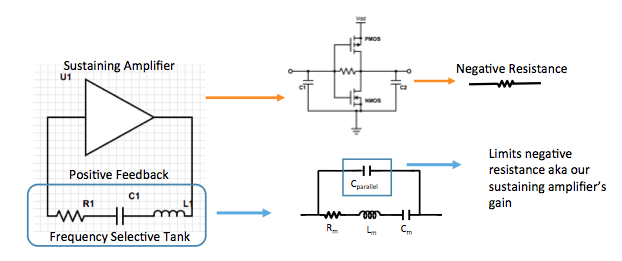
In this chip, there are two oscillator circuits: an inductor and capacitor (LC) oscillator and a ring oscillator. The ring oscillator was analysed and designed using the RC delay of digital theory, meaning the delay of a single stage decides how many stages of the same circuit are needed in order to obtain the desired frequency. The methodology used to design the LC was the negative resistance approach .The idea is the oscillator can be simplified into two main components: an amplifier (negative resistance) and a frequency selective tank. The frequency selective tank, as the name says, picks the desired frequency (f=1/(2*pi*sqrt(LC)) and passes it on to the amplifier. This cycle is repeated constantly, if the gain of the amplifier is large enough to compensate the losses in the resistance of the circuit, the output will be a sustained oscillation. Put simply for a system to oscillate its gain or negative resistance must be equal or greater than the equivalent resistance seen by the amplifier. For oscillation the gain of the amplifier has to be large enough to cancel out the losses of the resonator (if in series R_neg > R_m, if in parallel R_neg < R_m). It is worth mentioning the Cparallel which refers to the parasitic capacitances of the circuit itself, will lower the equivalent Rneg, this is because at higher frequencies the capacitor will behave like a short circuit and will feed forward, effectively cancelling out any resistance in parallel with it.
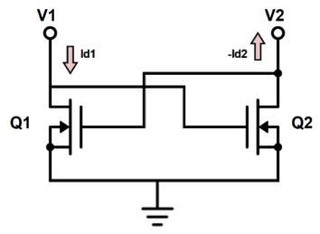
We now move onto computing the negative resistance of the topologies. By removing the resonator (frequency selective tank), we are left with the amplifier stage as shown in the following figure.
By connecting a test voltage supply at the inputs where the filter would be, we can write equations that allow us to derive the gain or negative resistance, as follows:
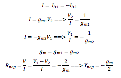
This is the resulting negative resistance for a pull down only network, for the compementary network used in this IC (PMOS+NMOS), the resulting resistances are in parallel, and hence it is easier to look at in admittance where they simply add up.