
Block Description

In the LC the resistance is not explicitly added, the resistance the circuit will face is the intrinsic loss of the inductor coil, this can be approximated after obtaining the LC values. To obtain the inductor and capacitor we first decided on a frequency of operation at 1.8GHz. Then the capacitor was selected to be greater than the parasitic capacitances of the transistors (approx. 400fF from simulations), the value chosen was 2pF. With these variables fixed now it is possible to calculate the inductance (f=1/(2*pi*sqrt(LC))=>L=1/(C(2*pi*f)^2 )), resulting in 4nH. With the extracted Q we could now compute the value of the intrinsic resistance of the inductor by Q=R_p/X_L =>R_p=Q*X_L. Now that we have the resistance we designed the negative resistance to be greater. The equivalent resistance of this circuit can be expressed as R_neg= -1/(g_mn/2+g_mp/2). The circuit was designed to operate in moderate inversion g_m/I_D ≈10, and for a WL limited to a parasitic capacitance of 400fF. To satisfy the first requirement a minimum I_D was selected hence I_tail=2I_D. For frequency variability the capacitor used is a varactor, controlled by a voltage Vc (0-1.4V).
Ring Oscillator
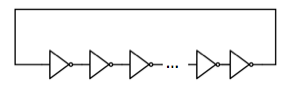
For the ring oscillator, we wanted a simpler test structure than the LC, this topology is useful for testing, any change in the system will cause a frequency shift and which we could ideally use for characterizing the future post-processing and its effect on the CMOS. Minimum length was used for these devices and a width of 5um for NMOS and 10um for PMOS was chosen. We wanted it to work around the hundreds of MGHz, the delay for one stage was measured to be 35ps so if f=1/(2*n*t) where n is the number of stages and t is the delay for a single stage, the frequency should be approximately 600MHz.
50-Ohm Buffer
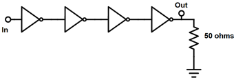
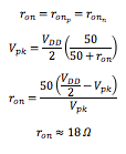
The oscillator outputs are to be measure on-chip using signal-ground-signal (SGS), for the differential outputs and ground-signal-ground (GSG) for single ended. These probes are matched to 50-ohms, therefore the buffers were designed for this specification. The power desired at the output is 3dBm which means a 2mW output. Then following the analysis:
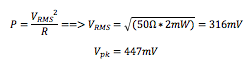
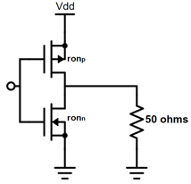
This would be the minimum voltage required at the output to drive the 50-ohm probes, with this it is not possible to calculate the on-state resistor value of the transistors in the inverter as follows.
Now with the help of simulations and assuming minimum length the widths can be extracted. Starting from the closest buffer to the output (right-to-left) each buffer before it will be 2.7 times smaller for optimum delay.
Level Shifter
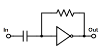
To ensure the signal is buffered correctly, the outputs of the oscillator were level shifted to oscillate around V_DD/2. The circuit has a decoupling capacitor at the input to strip the DC part of the signal. The resistor across the input and output terminals of the inverter is large (MΩs) no current is ideally flowing through it, its only purpose is to fix the input and output at the same voltage level V_DD/2. The output of this stage goes into the buffer.