
Testing
With the PPG6350 chip and the PCB in hand, the testing procedures started.
First the bonding wires from the die to the IC
package as well as the power supply vias on
the PCB were verified. Then the verification of the chip DC operating point and functionality of separate blocks was performed. The functionality test was first checked with waveform generator and then the actual fingertip was used to generate the PPG signal. Finally the
functional tests were done with the PCB.
After the bonding wires were checked, the testing procedures were started with the breadboard.
Breadboard Test
To make sure the DC operating points of OTAs were right, first the power supply was set to 1.8V, common mode voltage Vcm was set to 0.9V, Vss was set to ground and the 25 uA current source was provided with a potentiometer, then a 0.9V DC voltage was fed into both the OTA positive input vi+ and negative input vi-. Measured the DC voltage level at the output and compared it with the simulation result 0.9V. Measurement results showed that the DC voltage at the first stage OTA output was 0.89V and the second stage OTA was 0.8V, so the DC operating points of OTAs were right.
Functionality test:
OTA:
The waveform generator was used to generate the sinusoidal waveform needed. Set Vdd to 1.8V, Vcm to 0.9V, Vss to ground, and provided a 25uA current source with a potentiometer at i_source. Applied a 2Hz, 20mV peak-to-peak voltage, and 0.9V DC voltage sine wave at the positive inputs of the OTAs and measured the output waveforms at the output.
The figure above showed the input and output signal of the first and second stage OTA. The figure on the left was the test result for the 1st stage OTA. The signal in yellow was the input signal, whose frequecny was 2Hz, Vp-p=19.8mV, and DC voltage was 901.56mV. The siganl in green was the output signal from the OTA, and its peak-to-peak amplitude reached 479,71mV and DC voltage was 852.67mV. The figure on the right was the test result for the 2nd stage OTAc, the frequency of the input signal, which was in green, was 2Hz, the peak-to-peak amplitude was 30.8mV and DC voltage level was 910mV. The signal in blue was the output signal from the OTA, which was the amplified version of the input signal, and its peak-to-peak signal reached 716mV and DC voltage level was 785mV. The actual gain of the second stage OTA was 27.33dB, compared to the simulation result 29.31dB, it worked very well. Because of the mismatch in the circuit, there was a DC level shifting of the OTA output.
Comparator:
Set Vdd to 1.8V, Vcm to 0.9V, Vss to ground, and provided a 25uA current source with a potentiometer at i_source. 2. Applied a 0.9V DC voltage at comparator reference voltage input Vref and a 2Hz, Vp-p=20mV, DC voltage=0.9V sine wave at the input Vin of the comparator. Measured the signal waveform at the output of the comparator.
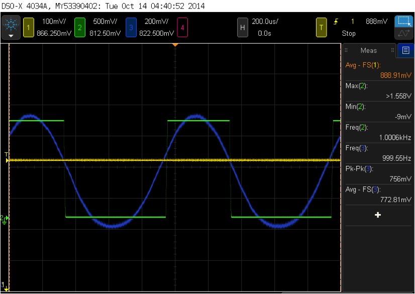
In the figure above, the signal in yellow was the reference voltage 0.9V. The signal in blue was the input signal and the green signal was the output signal. The comparator worked well with the sine wave.
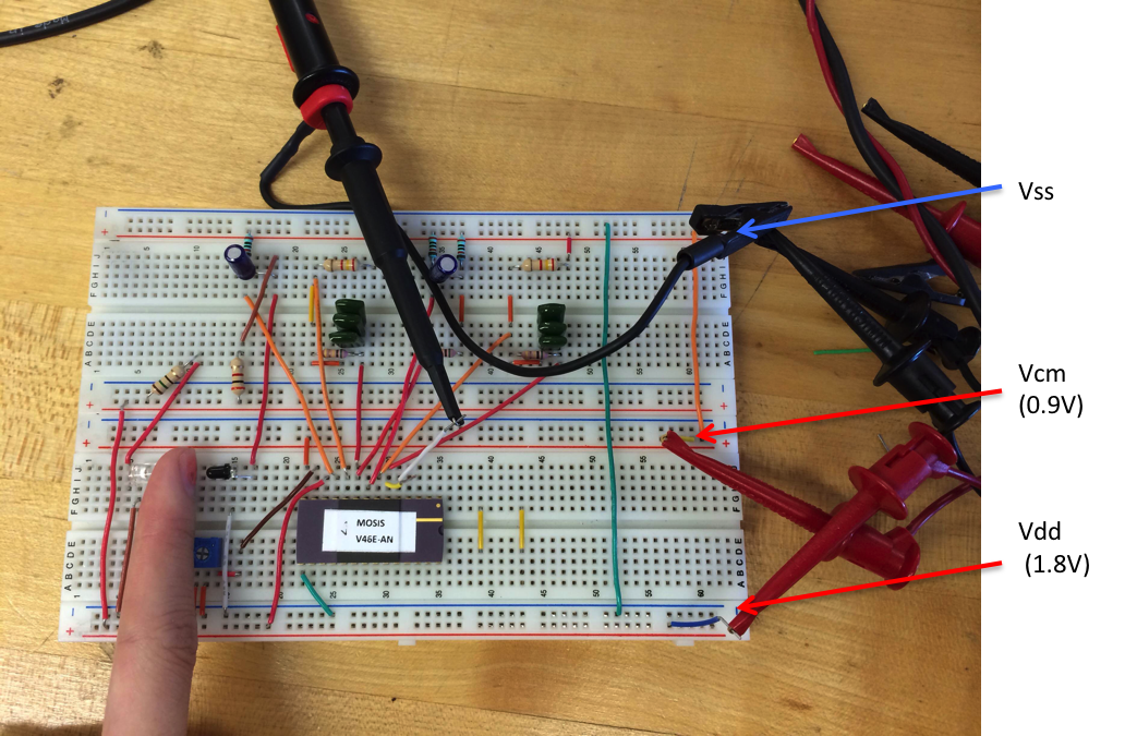
Finally the fingertip was used to generate the real PPG signal. Below is figure for the breadboard setup.
Test results:
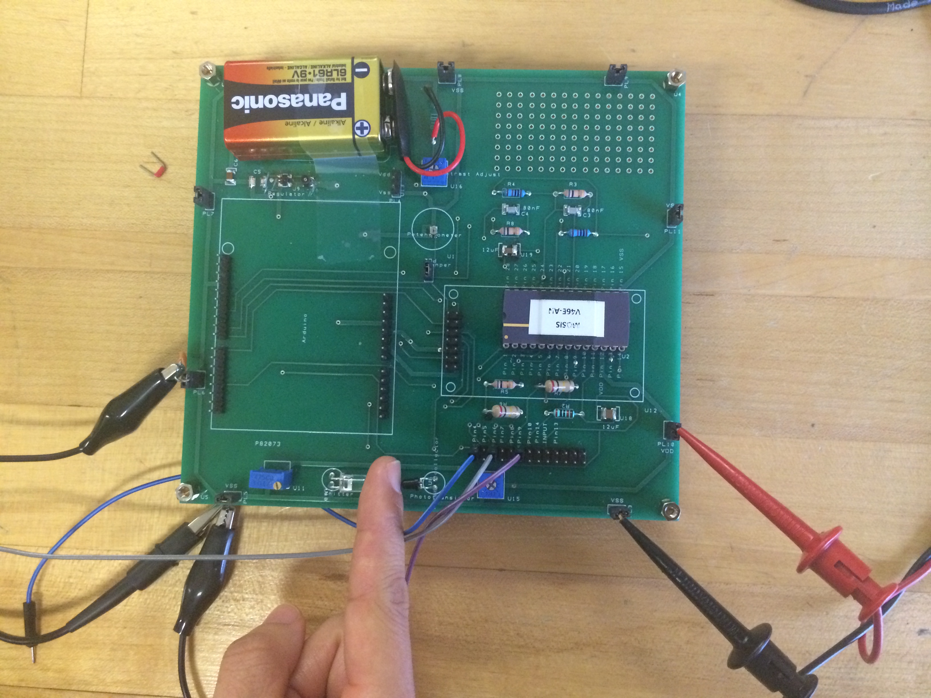
PCB Test
After confirming the functionality of the chip was right, the PCB test was performed. The test started without the Arduino and LCD display. Below are the pictures of the PCB setup and test results.
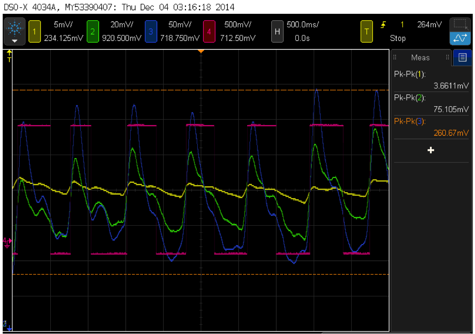
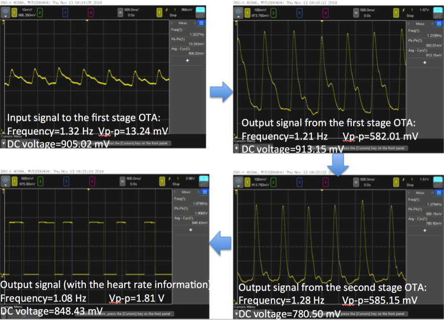
The figure above shows the PCB test results. The yellow signal represents the input signal to the chip, the green signal is the output of the first stage OTA, the blue signal is the output signal from the sencond stage OTA, and the pink signal is the final output from the comparator, which is synchronous to the heart rate.
At last, the Arduino and LCD were configured to process the comparator output signal and calculate the heart rate every 10 seconds, then display the result on the LCD screen. Below is the demo of how the heart rate monitor chip works.
