
System Overview
There are mainly five parts in the Heart Rate Monitor system: the PPG signal generation part, the high-pass filters, the first stage amplifier with low-pass filter, the second stage amplifier with low-pass filter, and the comparator.
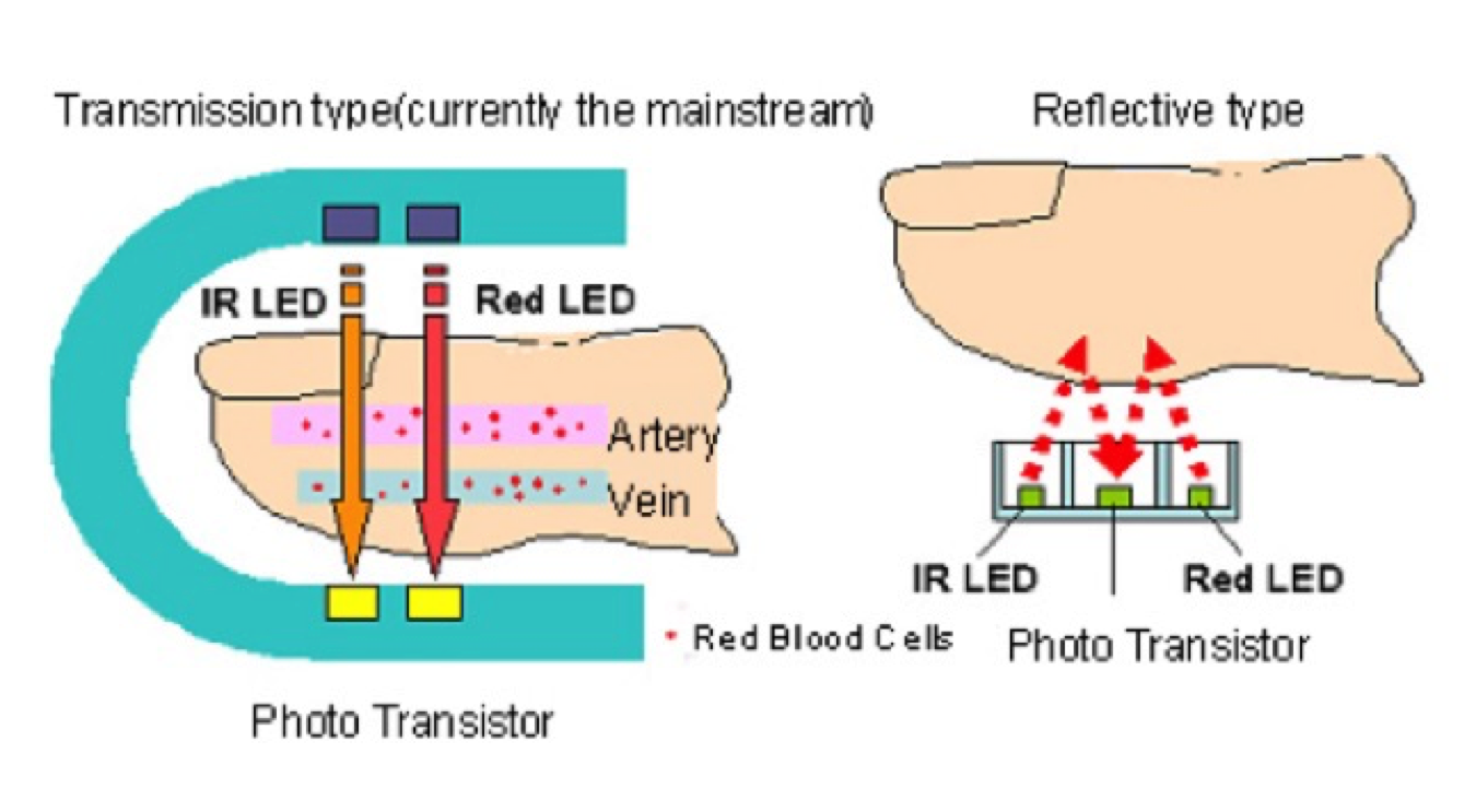
The PPG signal is generated by an infrared LED and a photodetector, and to monitor the heart rate, a finger must be put between the LED and photodetector. The infrared LED used in this project is the LTE4208 and the photodetector is the LTR4206. The change of the blood volume with heartbeat causes the small changes in the current of photodetector and results in a series of periodic pulses. A plot of this signal against time is the PPG signal. There are mainly two types of ways to detect the PPG signal, the transmission type and the reflective type, as shown in the figure below.[2] In this project, the transmission type is used.
The input PPG signal to the chip contains both AC and DC components.[3] The AC component is mainly caused by pulsatile changes in arterial blood volume, which is synchronous with the heartbeat. So the AC component is the useful part which contains the heart rate information. The DC component relates to the tissues and the average blood volume, so it is unrelated to the heart rate. The DC component of the PPG signal needs to be filtered out by a high-pass filter just before the PPG signal feeds into the chip. And the AC component of the PPG signal is only a small portion of the whole signal, so an effective amplifer is needed to amplify the desired signal and extract the heart rate information from it. So the main task of the chip is to amplify the signal and filter out the interruption noises caused by respiratory activity or motion artifacts. The output signal feeds into a microcontroller Arduino Uno Rev3, which counts and calculates the heart rate and display it on the LCD display. The system architecture is shown below.[1]
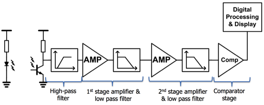
The frequency spectrum of motion artifact (MA) corrupted PPG signal includes different frequency components: the pulsatile (cardiac) portion (0.5-4Hz) and its harmonics, respiratory activity (0.2-0.35Hz) and motion artifacts noise component (0.1 Hz and more)[1]. So we need high-pass filters (cut-off frequency is set to 0.5Hz) and low-pass filters (cut-off frequency is set to 4Hz) to filter out the interruptions. The two-stage amplifiers will amplify the small input signal to the amplitude that can be detected. Finally the amplified input signal goes into a hysteresis comparator to convert the analog input signal to digital output pulses, which have the same frequency as the heart rate. Then this signal feeds into the Arduino Uno board for signal processing and display the heart rate on the LCD screen.
Building Blocks
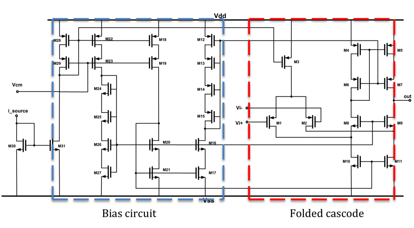
The main building blocks of the heart rate monitor chip are two operational amplifiers (OTA) and a hysteresis comparator.
OTA:
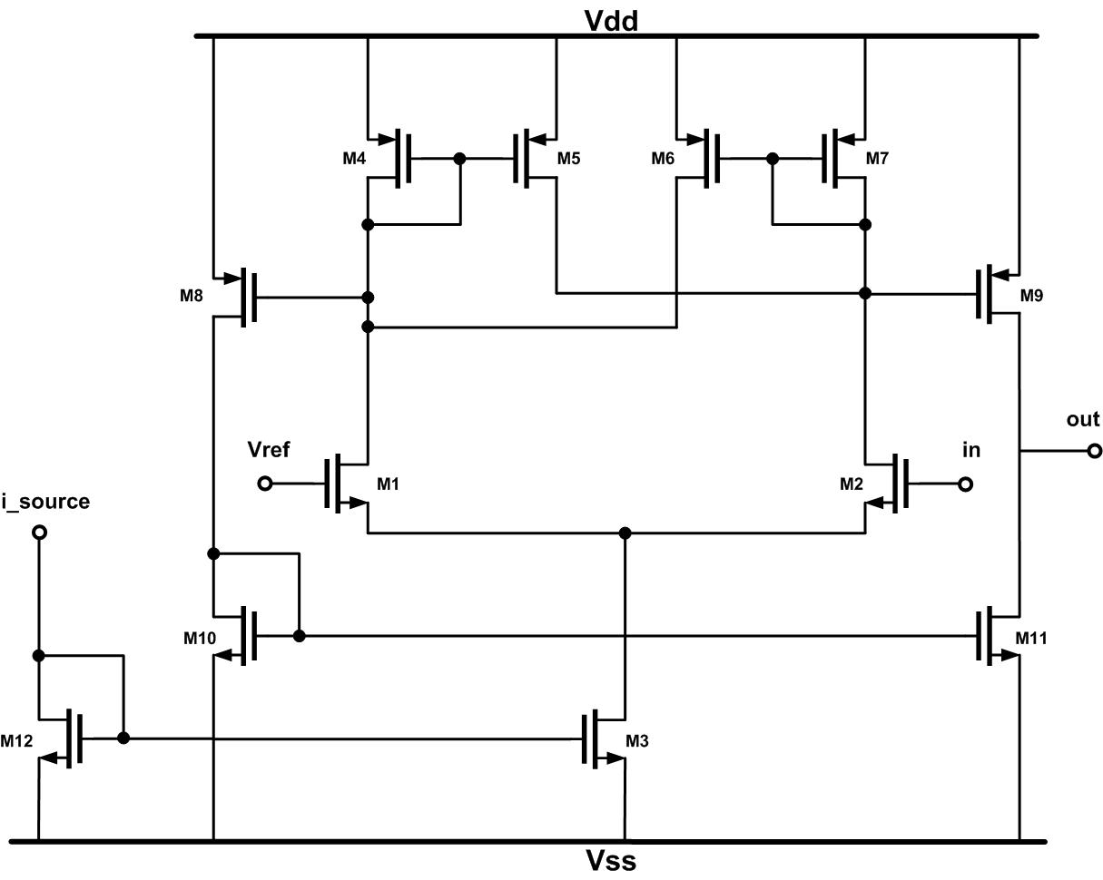
The folded cascode OTA structure is used in the design for several reasons; first of all, to make sure the circuit works as well as possible, a second stage is avoided, so the folded cascode structure can increase the gain the OTA to a large extent; second, it has self-compensation without the need of a compensation capacitor, so it is reliable and less susceptible to manufacture variations; third, it usually has relatively low power-dissipation, which is important for this application of heart rate monitor, since it is designed to be portable and durable.
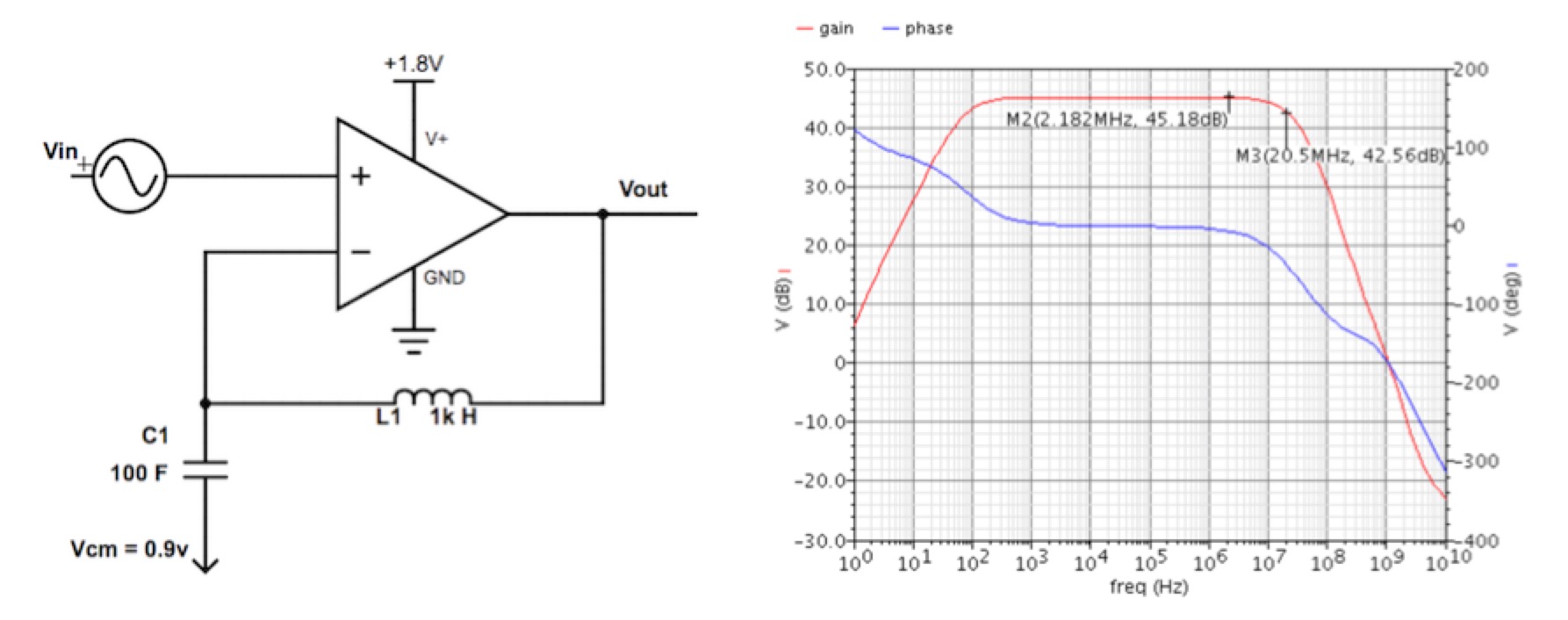
Schematic design:
Simulation results:
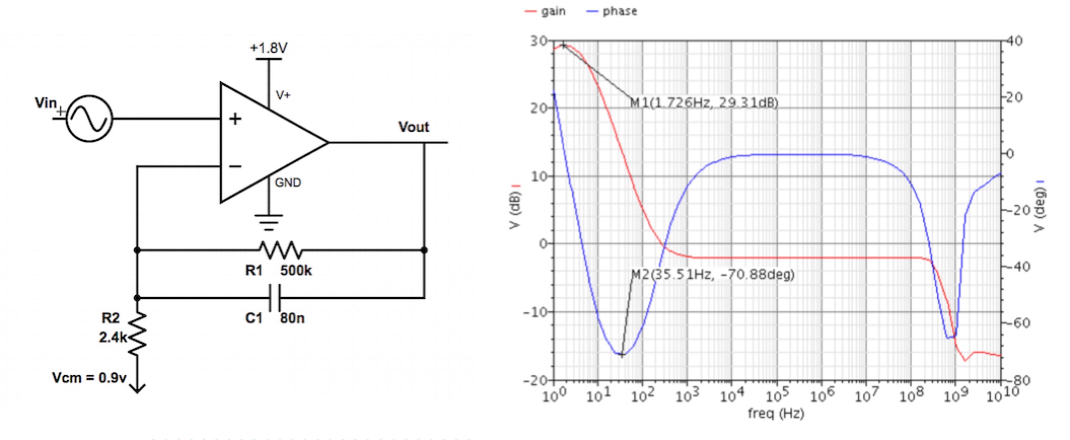
Open loop:
Closed loop:
Comparator:
Since in this heart rate monitor application, there are a lot of noises, so to suppress the influence of noises on the application, a hysteresis comparator is required. We use a simple comparator with internal positive feedback as our hysteresis comparator structure[4]. The hysteresis of the comparator is 50mV.
Simulation result:
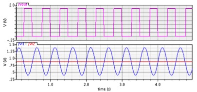
We apply a sine wave at the input of the comparator with DC voltage of 0.9V and the reference voltage is set to 0.9V, then observe the output signal.
System Implementation
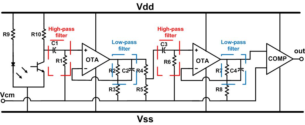
Below is the detailed implementation of the whole heart rate monitor system.[5] The input signal first goes through a high-pass filter with cut-off frequency of 0.5 Hz, and eliminate the low frequency signal. Then the signal goes to the first stage amplifier, whose closed loop gain is set to 34 dB. A low-pass filter follows the amplifier with cut-off frequency of 4 Hz. After the first stage OTA, there is a potentiometer that can adjust the voltage gain. The signal then goes through another stage of amplifier with low-pass filter. Finally, the output signal of the second stage OTA feeds into a hysteresis comparator with the reference voltage set to 0.9V.
Simulation result:
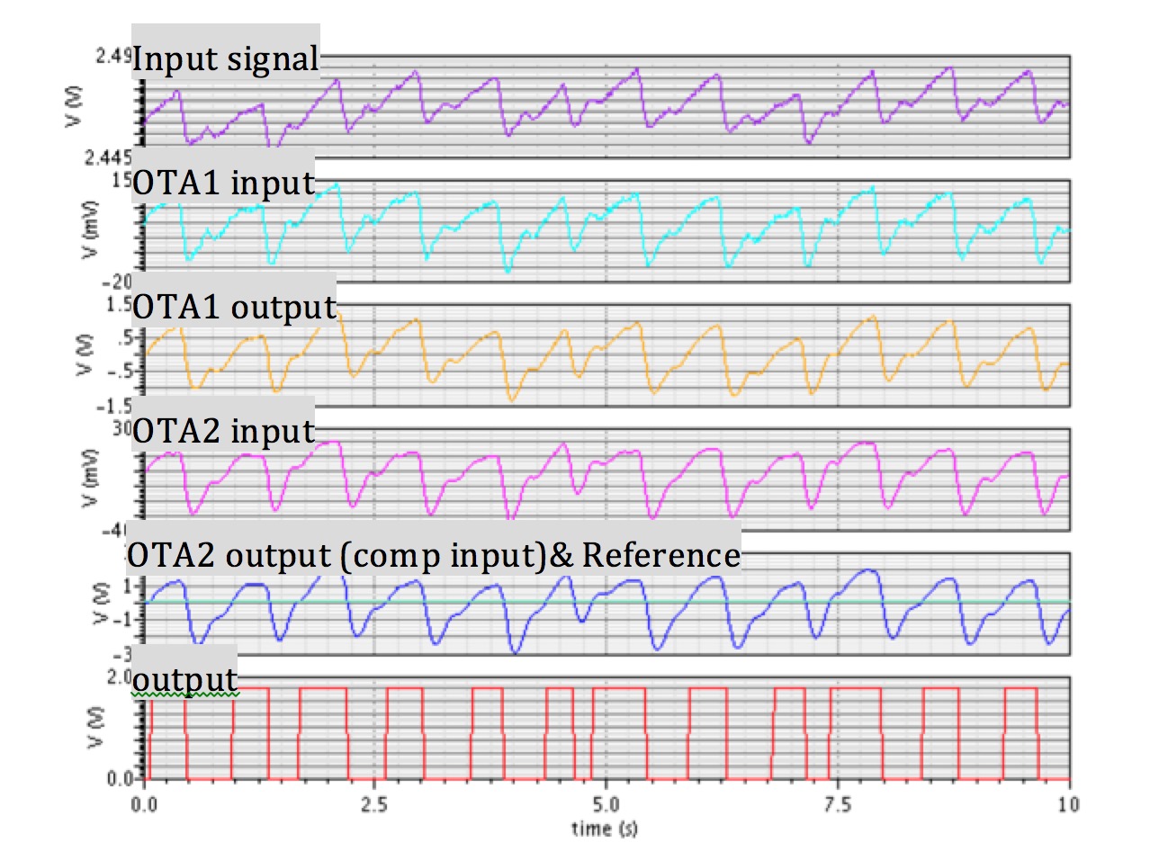
The heart rate monitor chip can filter out the unwanted information of the input PPG signal, amplify the useful heart rate information and generate the square wave which has the same frequency as the heartbeat. This digital signal is then fed into the microcontroller for signal processing to count and calculate the heart rate.