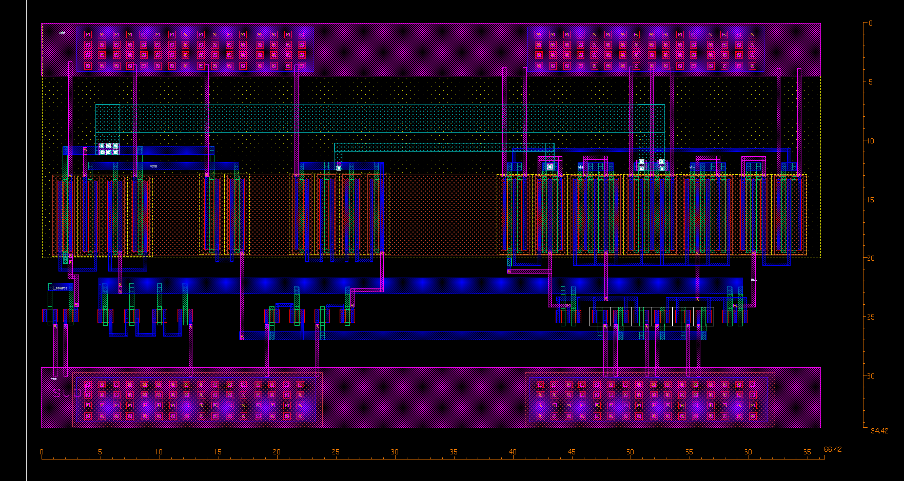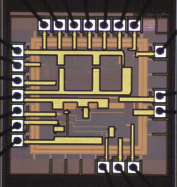
IC Layout
The figure below shows the layout and die photo of PPG6350. We also integrate another PPG chip in our design. The signal flow is from left to right, and the three main blocks are distributed along one side of the die to minimize the trace resistance to the pins. We use 12 pins, one VDD pin and one ground pin.