System Design
A Pixel and It's Subcomponents
The photodetector chip has 40 pixels, while some are connected via a decoder, directly outputed to a pin, or in a "test pixel" configuration, they all use the same general architecture:
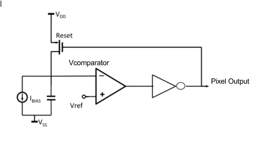
Photodiode
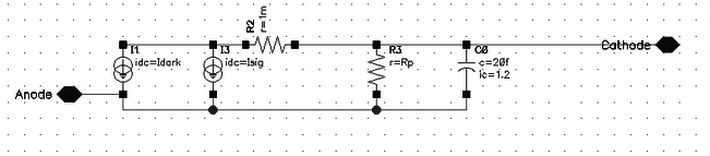
Each photodiode must be coupled to its own integrator/comparator circuit, because of this high amount of integration size is critical and the width must contain both the photodiode and the pixel control circuitry since both the photodiode and control circuitry are implemented in the silicon layer. Photodiode dimensions of 100um by 0.5um were chosen for the above reason. A photodiode area of 100um by 0.5um leads to a parasitic capacitance of approximately 1fF [2]. The photodiode can be modelled as a current source in parallel with a parasitic resistance and capacitor. During design, to estimate the expected photo-diode current output, we assumed a minimum illumination intensity of $\dfrac{1uW}{cm^2}$ From published literature, photodiodes fabricated in standard CMOS processes have demonstrated measured conversion efficiencies of $\dfrac{0.378A}{cm^2}$ [2]. With an active area of 100umx0.5um as mentioned above, the minimum photodiode output current is therefore, one can expect an output current magnitude of approximately 0.2pA.
Comparator
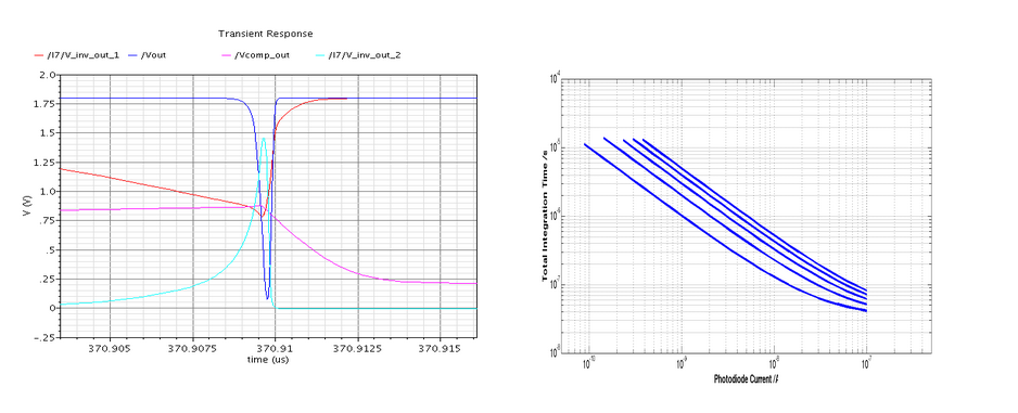
The core of each pixel circuit is the integrator/comparator block. The integrator integrates the output current of the photodiode over a specified integration time. Once, the output of the integrator crosses a threshold set by an external analog voltage reference, a count is triggered in a digital counter and the integrator is reset The output of the integrator is defined by $\int_0^Tint\dfrac{Iin}{Cint}$ . For a constant input current, the output voltage is given by $Vout=\dfrac{Iin*T_{int}}{C_{int}}$ Therefore, it is clear that the degree of signal amplification (transimpedance gain) is directly determined by the magnitude of the integration capacitor and the integration time. From the above minimum current limit of 0.2pA, combined with an integration capacitor of 200fF and an integration time of 1s, the output voltage is 750mV which can easily be discriminated by a comparator circuit.
The comparator block was implemented as an uncompensated two-stage OTA. The initial stage is a high-speed differential amplifier followed by a high-gain stage. For this particular application, the key metrics for comparator design are :
- High speed: The maximum speed at which the circuit can operate places a limit on the maximum current output that can be tolerated from the photodiode in response to illumination. Consequently, the speed of the circuit places a bound on the maximum dynamic range of illumination (i.e photodiode current)
- Size: Since, the goal of this application is to construct images for compact spectrometers, it is beneficial to make the pixel size as small as possible.
- The comparator is the only “analog” block requiring DC bias, and hence consuming static power. As a result, minimizing the required bias current for the comparator based OTA is necessary to reduce overall power consumption.
- Low-DC offset: Since, large arrays of pixels are envisioned, it is beneficial to ensure that each pixel (and hence each comparator) operate with the same comparator thresholds. The design of the OTA comparator commenced with a slew-rate specification derived from the expected loading capacitance on the output of the comparator. This yielded a slew-rate estimate of 1,000,000 V/second. With a the slew rate specification, the devices were all sized accordingly. The devices are all 300nm in length, since further increases in length did not yield substantial improvements in output resistance for the additional size penalty incurred with a longer transistor length. The W/L ratios of the various devices were initially chosen based on the slew rate specification and by selecting an overdrive of 200mV for all devices. An additional design goal was to keep the input common mode range as large as possible to enable the comparator to operate with a large range of reference voltages. After subsequent simulations and tuning of transistor sizes, the final design shown below was found to yield a satisfactory trade-off between device size and input common mode range (0.8-1.5 volts). Additionally, OTA design incorporated cross-coupled feedback transistors to improve the slew rate using positive feedback. The design was simulated under varying process corners (TT,SS,SF,FS) and no degradation in the switching behavior was observed due to 'latching' effects stemming from positive feedback.
Inverters
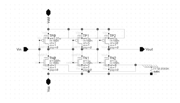
The switching output of the comparator is then input to a buffer comprised of three cascaded inverters. The output from this buffer subsequently drives the reset which charges the photodiode capacitance and restores it to its original value, thus resetting the pixel. The inverters are of progressively increasing sizes, with each stage four times the width of the previous stage. The buffer serves two functions. The current gain from the inverters sharpens the pulse output from the comparator which enables a fast pixel reset and improves capacitive load driving capability.
Buffers
The design incorporates seven full pixels that are directly connected to external chip pins and can be read directly. However, to demonstrate larger arrays of pixels, the decision was made to implement a multiplexing scheme whereby one pad can be used to read out the stage of multiple pixels connected to that pad. In order to enable multiple pixels to independently drive a shared pin, tristate buffers were added to the output of each pixel. The tristate buffer follows the three inverter buffer described above. The layout and schematic of the chosen tristate buffer design is shown below.
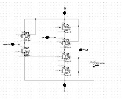
When the enable input of the tristate buffer is driven low, the output of the buffer switches to a high-impedance state. As a result, bank multiple pixels can use shared line individually and without contention. Additionally, the tristate buffers provide current gain, thereby enabling the pixels to drive large capacitive loads (up to 10pF at 10MHz switching frequency). This capability is necessary, since there is no onboard counter, therefore the pixel outputs need to be routed externally through the chip pads and to an external counter (or oscilloscope for testing), in which case the output signal could potentially incur large parasitic capacitances.
Current Distribution Network
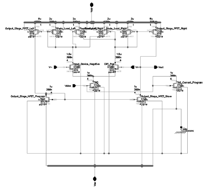
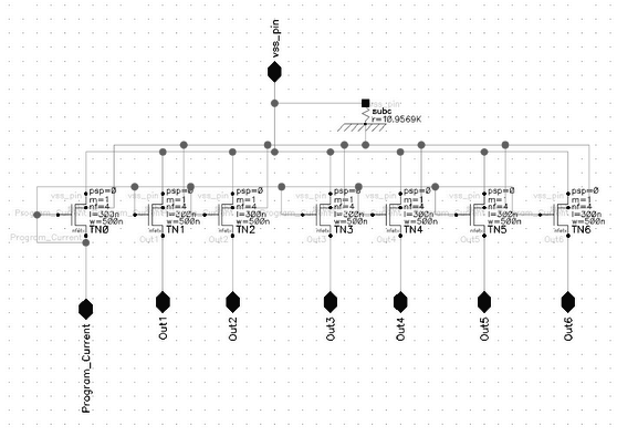
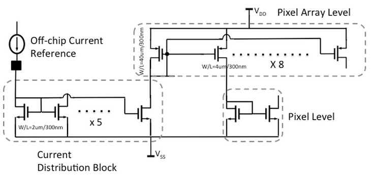
Each pixel requires a bias current for the tail current mirror in the OTA-based comparator. The chip contains 40 pixels in total, each requiring a bias current signal. In order to ensure individual pixel operation is as identical as possible, each pixel has a local current mirror. The overall bias current flow is depicted in the block diagram below. An off-chip bias current reference is applied to one of the chip pins. This is replicated five times using a current distribution block.The transistors in the current distribution block were chosen to be relatively small (W/L=2um/300nm) in order to increase overdrive voltage (Vgs-Vt) and reduce their sensitivity to threshold voltage fluctuation each corresponding to one array of pixels. The replicated current is subsequently applied to bank of pFET current mirrors which dividers the current by 10 and replicates it 8 times corresponding to the number of pixels in each pixel array. Finally, the divided current is applied to the bias tail transistor of the OTA based comparator in each pixel.
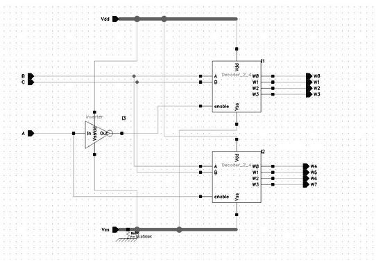
Decoder
The decoder was constructed using two, 2-4 decoders. The purpose of the decoder is to allow the user to select which pixel banks are sent to the pixel bank output pins. This is performed via the 'A B C' selection pins and internally via the enable lines on each pixel buffer.