
PCB Design
For testing, a variety of boards were made before the final PCB was fabricated. Shown below are the PCB schematics and layout.
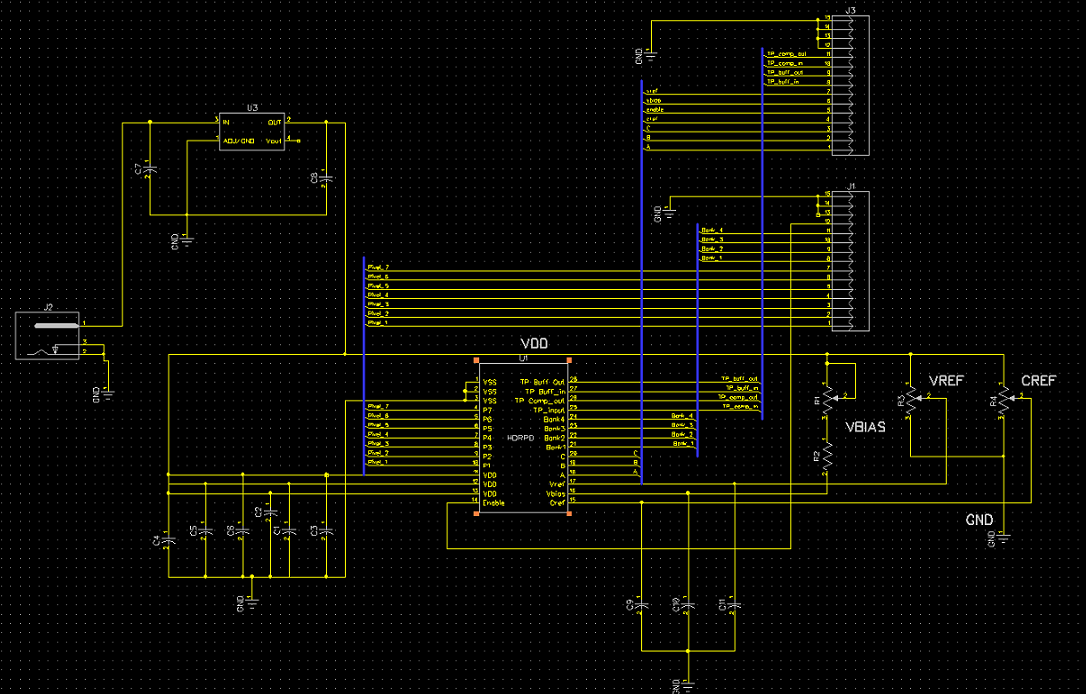
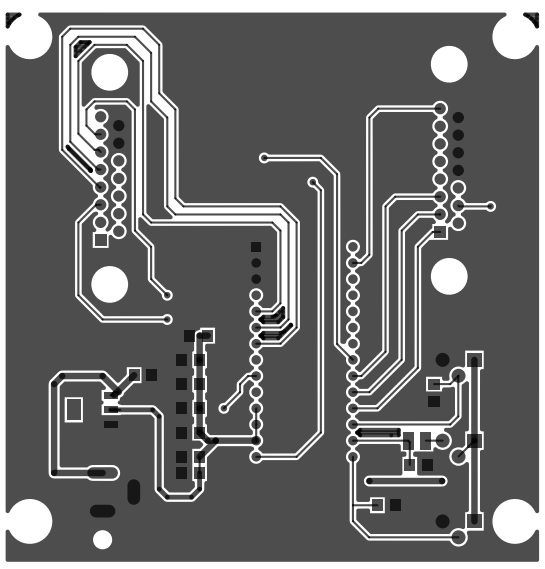
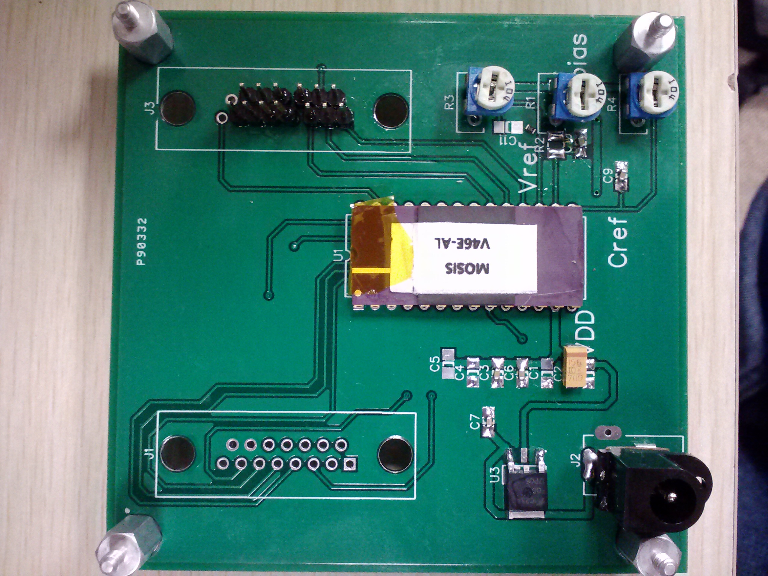
For testing, a variety of boards were made before the final PCB was fabricated. Shown below are the PCB schematics and layout.