
Test Results
During testing, each block's transient and AC gain measurements were taken using an Analog Devices ADALM2000 and a benchtop oscilloscope. The results for each block are reported below.
Individual Block Testing
Low-noise Amplifier
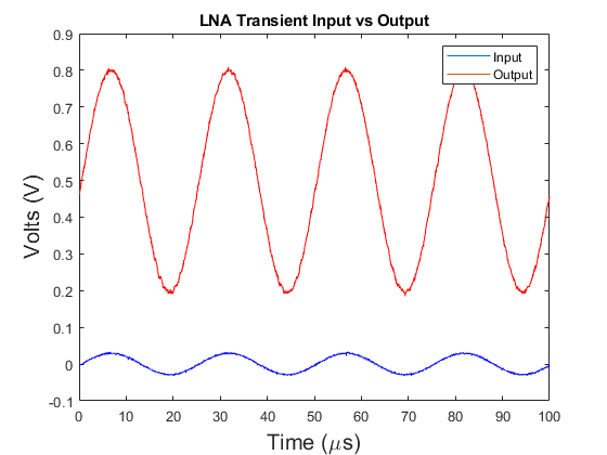
To test the LNA input block a transient 60mVpp 40kHz waveform was placed at the input of the AFE. The output transient waveform was measured at 600mVpp, about a 20dB gain. This matches the designed simulation. Additionally, the output waveform has a 500mV DC offset. The DC bias point for the rest of the stages in this chip are at 500mV, or Vdd/2. Fig. 1 below illustrates the transient result of the LNA, taken with a benchtop oscilloscope.
Analog Multiplexer and Single-ended-to-Differential Converter
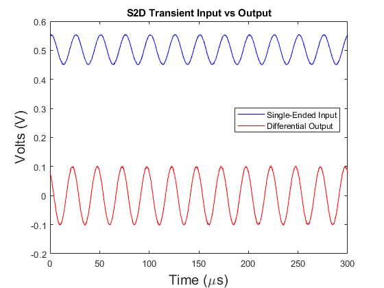
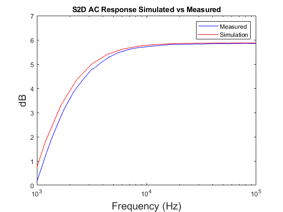
After the LNA and the CA inputs, the signal travels into a MUX that selects which input moves forward. The "0" state is the LNA input and the "1" state is the CA input. Moving into the single-ended to differential converter (S2D), is then transformed into a differential output at a 500mV common mode voltage. In Fig. 2 the transient single-ended output (blue) and the differential output (red) are shown. The single-ended input comes from the output of the mux which has a 100mVpp 40kHz signal with a DC offset of 500mV. At the output, the differential signal has a 200mVpp output voltage. This comes out to an approximate differential to single-ended voltage gain of 6dB. To verify this, the AC response was measured using the ADALM2000 2-port network analyzer, which is shown in Fig. 3. In the constant gain region, the measured and simulated gains show good agreement where the average gain is around 6dB.
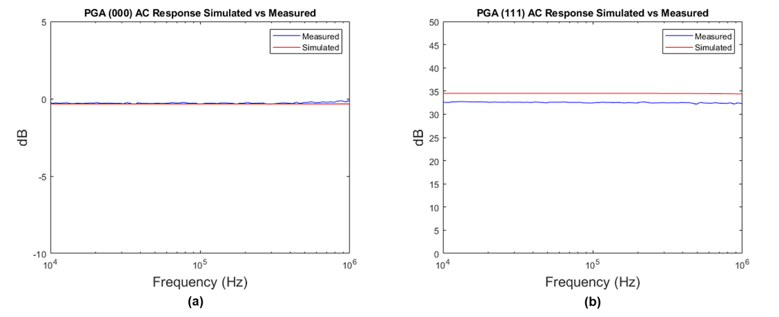
Programmable-Gain Amplifier
For the PGA testing, the transient outputs for all 8 possible gain states were measured. For simplicity, the lowest gain setting 000 and the highest gain setting transients are shown. For the 000 gain setting an input differential signal at 40kHz 160mVpp was set at the input of the PGA. Since the 000 gain setting was designed to be approximately 0dB gain, both the input and output signals are approximately the same. Fig 4 below illustrate the transient result of the PGA with the gain setting of 000 and 111, taken by a benchtop oscilloscope.
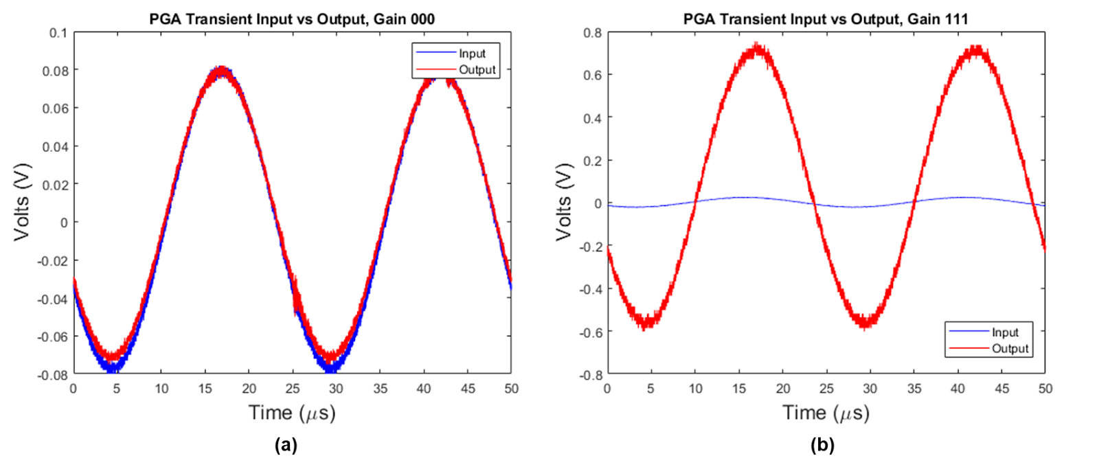
Fig. 5 below show the measured vs simulated AC response of the PGA with 000 and 111 gain settings.
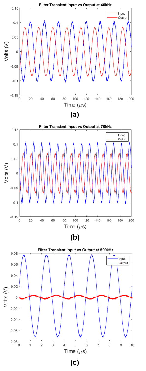
Filter
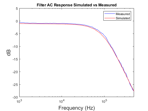
To test the filter, three different transient waveforms were placed at the differential input of the filter. The first was a 40kHz, 200mVpp sine wave that is plotted in Fig. 6a. As expected from the simulation, the pass band gain of the filter is below unity and thus the output voltage has a lower peak to peak magnitude than the input voltage. At our designed cutoff frequency of 70kHz, the gain hits an approximate attenuation of -4dB and at 500kHz, the output is attenuated by about -40dB, as shown in Fig. 6b and Fig. 6c, respectively. These values show in the transient response as the output signals continue to decrease as the input frequency is increased. Additionally, the AC response of the filter was measured using the ADALM2000 2-port network analysis. The results are shown in Fig. 7. The simulated model assumed a TT process corner with the IBIAS_FILTER variable resistor set to 6.5k to match the process testing of the fabricated chip.
Full Analog Front-end System Testing
Voltage-Based Sensor Signal Chain
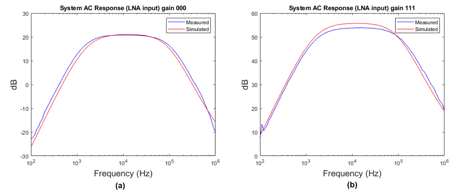
During the full system testing, a signal (voltage or current depending on the input) was generated at the input of the AFE and the output was differentially measured at the output of the filter. For the LNA, the differential to single-ended gain was measured for both the 000 (min gain) and 111 (max gain) states. Fig. 8a shows the minimum gain at 20.76dB in the pass band with an approximate high frequency 3dB cutoff at 73kHz. The maximum gain state of 111 is shown in Fig. 8b with an approximate gain of 53dB and a 3dB cutoff frequency of 73kHz.
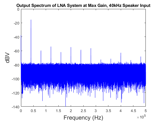
Looking at the output spectrum at max gain setting of 111, illustrated in Fig. 9, the largest peak is at the 40kHz input signal as expected. The SFDR from the signal tone to the highest spur is 38.9dBV.
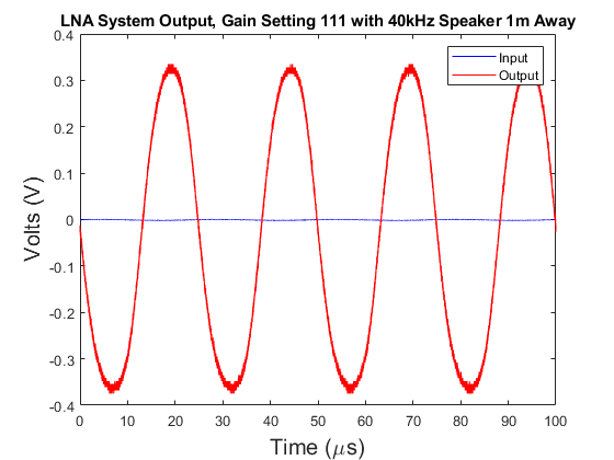
To test how well the AFE performed with a sensor input, a Murata MA40S4S 40kHz ultrasonic transducer was used as both the transmitter and receiver for the system. A 40kHz 1Vpp sine wave was inputted to the speaker side and moved 1m away from the AFE receiver. At the max gain state (111), the transient input and output is shown in Fig. 10. As the transmitter was very far away from the receiver, the raw voltage induced at the input was very small as shown. However as the signal moved through the AFE, the added 53dB gain, high and low frequency filtering, and differential protection from common mode noise led to a cleanly amplified differential output.
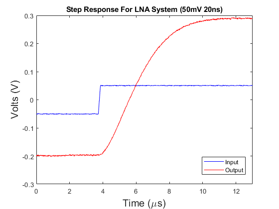
To measure the test response of the system and check for any possible instability, we put a small step function of 0 to 50 mV with a rise time of 20ns at the input of the LNA and observe the output signal. The result, plotted in Fig. 11, shows that the voltage-based sensor signal chain system is indeed stable, with no ringing or oscillation found at the output
Current-Based Sensor Signal Chain
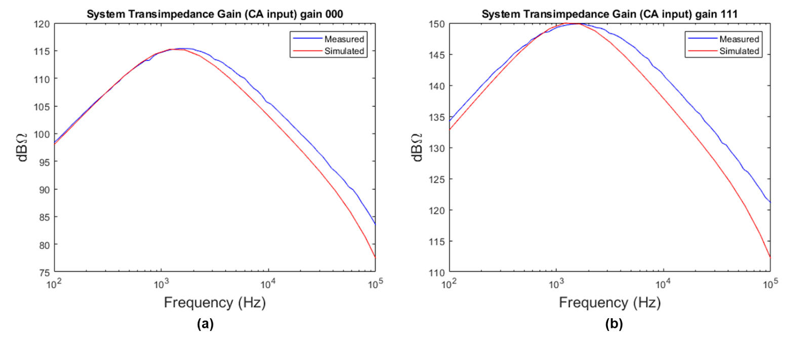
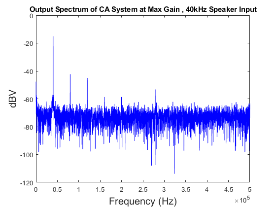
For the CA, the differential to single-ended transimpedance gain was measured for the 000 (min gain) and 111 (max gain) states. Fig. 12a and 12b show the range of peak transimpedance gain is between 115dBΩ-150dBΩ. Unlike the LNA response, the CA system output is an integrator and thus has a -20db per decade slope in its region of operation This region was designed to be 10kHz (set by the feedback resistor and capacitor) to 70kHz (set by the output filter). From the output spectrum in Fig. 13, the SFDR from the signal frequency to the next highest magnitude tone is 27.2dBV.
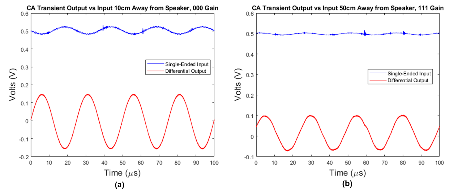
To test how well the AFE performed with a sensor input, a Murata MA40S4S 40kHz ultrasonic transducer was used as the transmitter while the receiver was realized with a custom designed PVDF-TrFE thin film piezoelectric sensor. A 40kHz 8Vpp sine wave was inputted to the speaker side and moved 10cm and then moved to 50cm away from the AFE receiver. As the sensitivity of the current-based sensor is lower than that of the Murata transducer, the gain needed to be increased at a shorter distance. For both the 10cm and the 50cm distances the max gain state was used. The resulting output voltage vs the input signal to the CA are shown in Fig. 14. An interesting observation is that the current based sensor has a wider bandwidth than the 40kHz murata receiver and thus the output voltage of the CA couples on more unwanted frequencies from the environment. Thus, the 70kHz low pass and the 1kHz high pass filtering is necessary to maintain the signal of interest.
ADC Testing
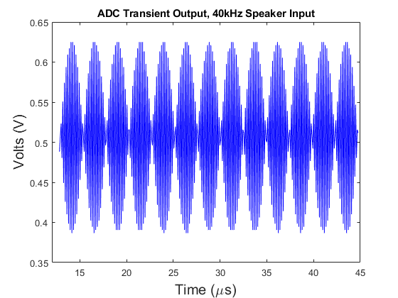
Our chip features an additional 8-bit SAR ADC, designed by Team 3: Doppelganger - Doppler Radar Receiver team. More details on the design of the ADC can be found on their website page. For the purposes of the ADC testing and integration with our AFE, the ADC was used to process and digitize the ultrasound input signals for our chip. Fig. 15. shows the transient waveform of the ADC output. The digital codes are transformed to analog voltages using an ideal DAC. We inputted a 40kHz sine wave with a 20mVpp amplitude from the voltage sensor input. The sampling frequency was set to 125kHz.
Using the LNA voltage input, a 40kHz sine wave with 20mV amplitude was generated by a function generator at a gain setting of 000. The differential output of the analog front end was AC coupled with the ADC differential input at a VDD/2 common mode voltage. With a sampling frequency of 125kHz, we collected the ADC output bits (B0-B7). After, we transformed the digital codes to analog voltages using an ideal DAC. Finally, we applied the FFT to the DAC output. Fig. 16 shows the result of the FFT. In this case, the ADC has a 2MHz clock.
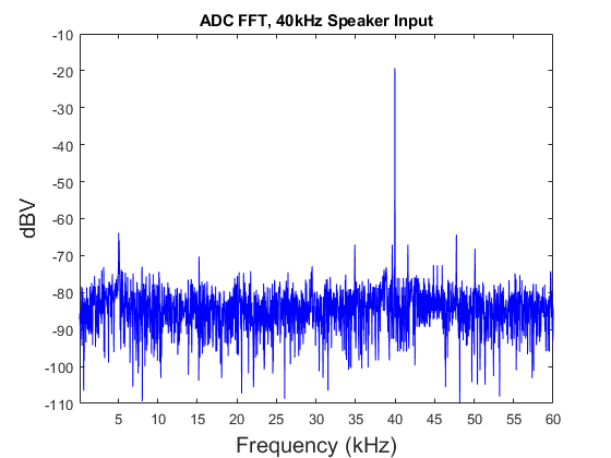
SFDR, which is the difference between first and second order harmonics, was calculated as 44.72dB. Signal to noise ratio (SNR) is the difference between input signal power and noise power, which was calculated as 40.41dB. The effective number of bits (ENOB) of the ADC was calculated as follows: ENOB = ( SNR -1.76 )/6.02 = 6.42