PCB Design
To bring up the full functional system, we design a 2-layer PCB which provides the connection between the IC and the required off-chip components. The PCB was designed using KiCAD
Schematic
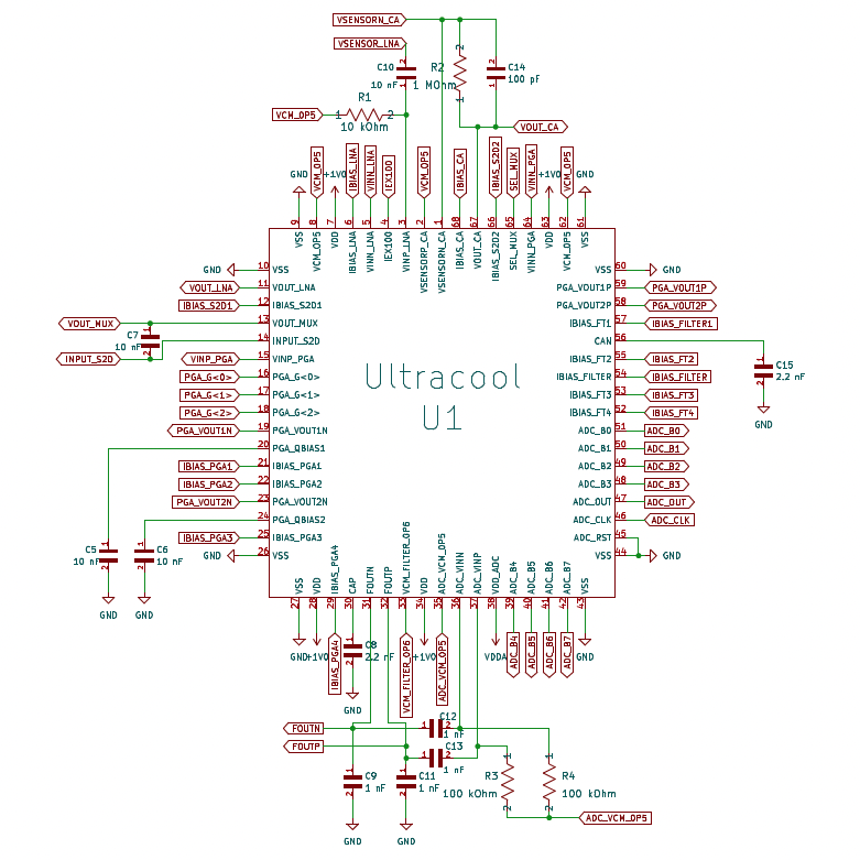
IC systems
We first build the schematic of the required passive components around the chip based on the system-level block diagram. Fig. 1 below illustrates the schematic of the systems around the IC
Supporting Subsystems
The supporting subsystems of off-chip components include 1V power supply for the 2 power domain - analog and ADC, common-mode voltage generator to provide the required 0.5V for most of the systems on chip and 0.6V for the filter, current reference, switches for digital control of PGA and multiplexer.
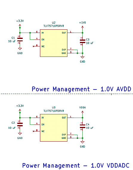
We use the TLV757P 1V low dropout regulator (LDO) to provide the power supply for the 1V analog power domain and the 1V ADC power domain. We use two different power domains to make sure that the noise in switching activities in the ADC does not couple into the analog domain through the power supply. The LDOs are supplied with 3.3V coming from the microcontroller being mounted on the board, which brings the total power domain in our board to 3. The schematic for the on-board power supply can be found in Fig. 2 below.
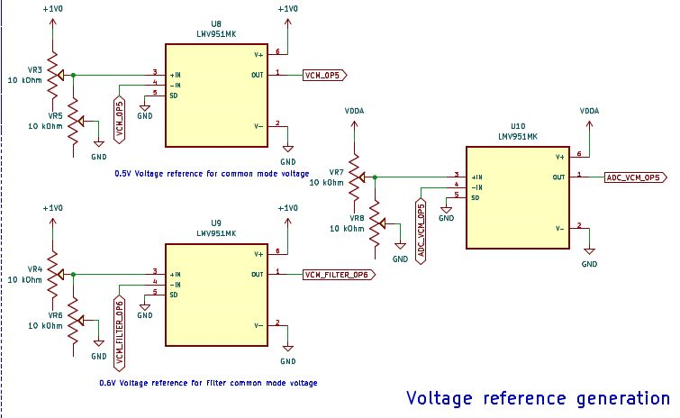
For the common-mode voltage generators, we use 2 potentiometers to form a voltage divider, and connect the output of this divider to a voltage follower circuit. The value of the generated common-mode voltage can be tuned by the potentiometer. These 3 circuits would provide 0.5V common-mode voltage for the analog circuitry and the ADC, and 0.6V for the filter.
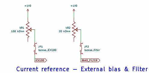
To generate the current reference for the current distribution block on chip as well as the current tuning to adjust the filter’s corner frequency, a potentiometer and a jumper are connected to the current bias pin on the chip as shown in Fig. 4. The potentiometer is used to adjust the current reference value, while the jumper is used to connect an ammeter to check the current reference value. The jumper would be shorted during normal operation of the chip
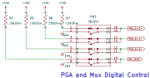
To provide the digital control for the PGA as well as the mux, we use a set of 2 way switches connecting to a pull-up resistor on one side and ground on the other side as shown in Fig. 5.
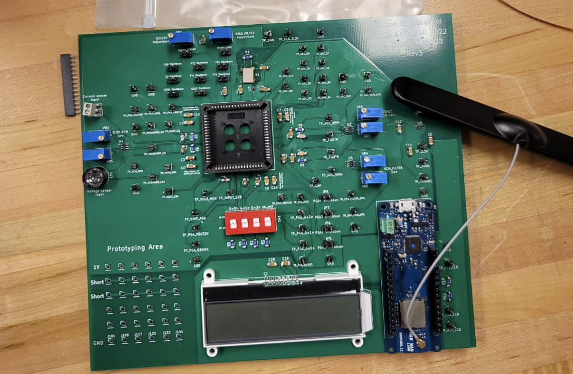
Additionally, various test points are added to access all pins on the chip and different nodes of the on-board circuitries for testing and measurement purposes. The board also features a prototyping area, which is basically a 6x6 grid of 2.54mm holes, so that extra through-hole components can be added later on for debugging purposes. Finally, we include a microcontroller board, an Arduino MKR WAN 1310, and an LCD display as part of the circuit board to perform data processing and display information.
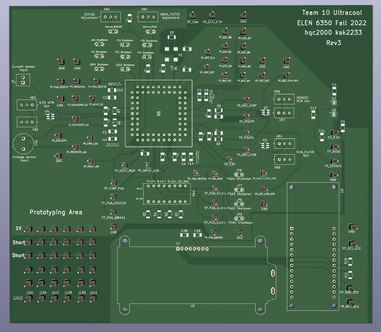
Full PCB Layout
The layout of the PCB (top layer, bottom layer and both layers) are shown in Fig. 6, 7 and 8. As previously mentioned, we have 3 different power domains in our board. Each of these 3 power domains are laid out using 3 different polygons on the top layer to ensure a low impedance on the power distribution network. The bottom layer of the board is covered by ground polygon. The prototyping area is placed in the bottom left corner of the board, with 1 row being connected to the 1V analog power domain, and each of the next 2 rows are shorted together. The area of our board is 150mm x 170mm
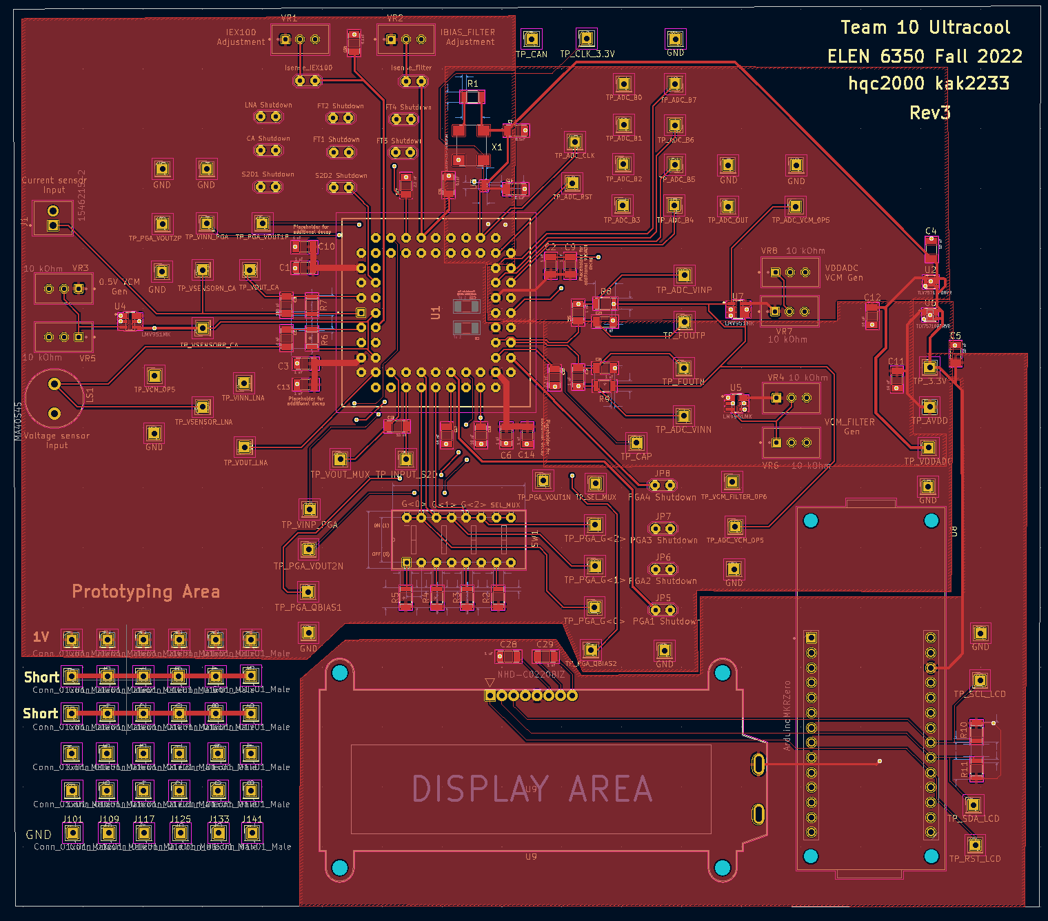
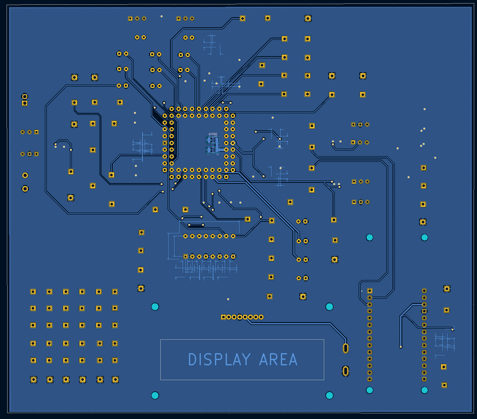
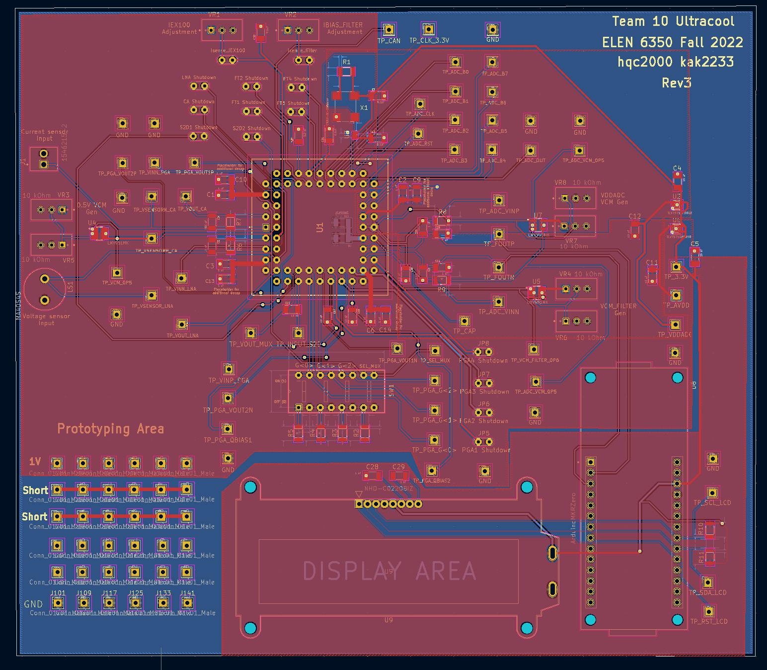
Fig. 9 below shows the 3D view of our board, and Fig. 10 shows the final form of our board after being assembled.