
Architecture
Filter Topology
The topology of the 4th-order Butterworth low-pass filter was developed from a passive circuit RLC prototype filter [3] using an active component replacement design method [2] resulting in the transconductor-C based implementation shown in Fig. 1. Prototype filter resistors are replaced with unity-feedback transconductors and inductors are replaced with transconductor-based gyrator-C active inductors.
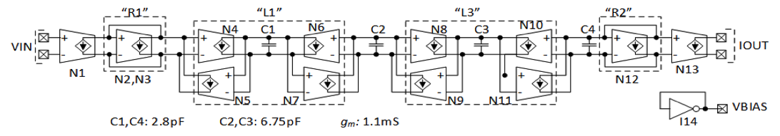
Fig. 1. 4th-Order Low-pass Butterworth Filter
Inverter-based Transconductor
Inverter-based transconductors [2] as shown in Fig. 2 can achieve high performance since they have no additional internal nodes. In terms of portability towards highly scaled processes with reduced supply voltages, the two-transistor stack inverter inherently supports low supply voltage operation [4]. The inverters are biased to operate in their linear region. The transconductance (gm) is produced by inverters N1-N2. The cross-coupled inverters, N3, N4, and shunted inverters, N5-N6, provide common-mode signal rejection and differential-gain enhancement. The complete transconductor is comprised of just two types of inverters with two different transistor widths; N5-N6 (19.4um PMOS, 3.88um NMOS) have widths 3% less than N1-N4 (20um/PMOS, 4um/NMOS). A single shunted inverter (I14) provides the common-mode reference voltage VBIAS for external interfaces and an output transconductor (N13) transforms the filter voltage output signal to a current signal so that the chip can be exclusively designed with Verilog and standard cells (see Fig. 1). For the measurements, the filter output current is transformed to a voltage with an external transimpedance amplifier.
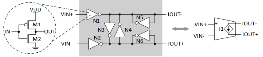
Fig. 2. Inverter-based Transconductor
Digitally Programmable Capacitor Trimming & Serial Interface
The pole frequencies of the various stages in the filter are set by ratios of transconductances and capacitor values. Chip manufacturing variations cause transconductance and capacitance variations that can alter the cut-off frequency (fc). After fabrication, these variations in fc can be compensated by altering the capacitances of the main filter capacitors with digitally programmable trim capacitors. Small trim capacitors can be selectively connected in parallel via transmission gates to each of the four main filter capacitors to trim the value ~+/-20% in eleven steps (see Fig. 3). The main capacitors are designed as 80% of the desired value and the trim capacitors provide a programmable range of 40%. The two distinct main filter capacitor values, 2.8pF and 6.75pF, are trimmed separately since trim values have a programmable resolution of 50fF. The 2.8pF and 6.85pF capacitors have trim capacitor banks of (1x 50fF and 11x 100fF) and (1x 50fF, 1x 100fF, and 13x 200fF) respectively.
A simple digital serial interface (see Fig. 3) controls capacitor trimming. A serial bit stream is shifted into the shift register. To simplify clock tree design, pipelined flip-flops are clocked on alternate clock edges to ensure adequate setup and hold timing based solely on clocking frequency. A synchronous load enable signal latches the trim capacitor control enables.
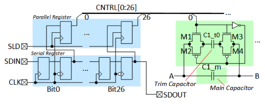
Fig. 3. Digitally Programmable Capacitor Trim Circuit