System Overview
Class-D amplifier is an efficient design which based on converting the audio signal to a pulse-width-modulation signal, a high power buffer stage, and finally, reconstruction of the audio signal back through a low-pass-filter stage. The block diagram of our design is shown in figure 1. It is a single channel amplifier with a gain determined by the ratio of the Rf and Rin resistors, build to drive an 8 ohm speaker. For the functional testing we designed an FM radio as an input to the amplifier.
The amplifier includes several building blocks, including Operational Transconductance Amplifier (OTA), comparator, triangle wave generator, non-overlap generator, output driver and output low-pass filter, as shown in Fig. 1. Note that Rin, Rf, L1, C1, C2 are all off-chip components.
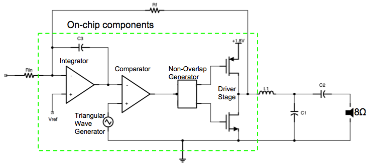
Fig. 1: Block diagram of the class-D amplifier
Fig. 2 shows the simulation results of the input and output signals. The input signal is a 5 KHz sine wave with a DC biasing voltage of 0.9 V and a Vpp of 400 mV. The output voltage is measured from the 8 ohm load resistor.
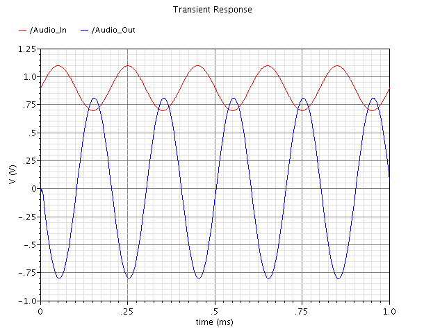
Fig. 2: Simulated input and output of the class-D amplifier
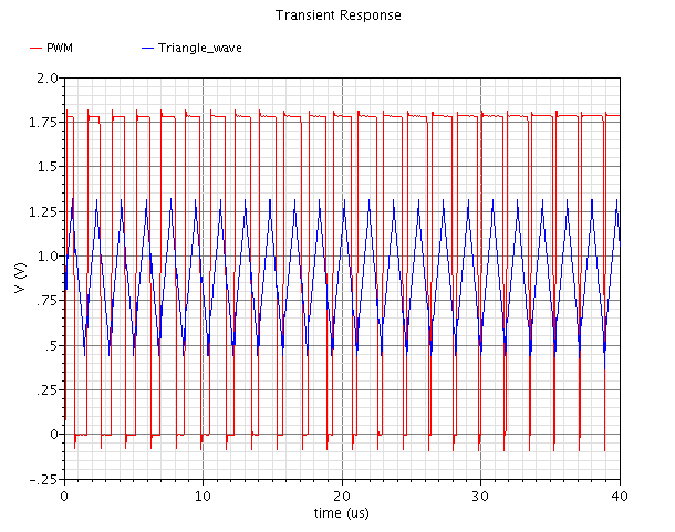
Fig. 3 shows the internally-generated triangle wave out from the triangle wave generator and the PWM signal out from the comparator.