PCB Design
We designed a two layer PCB board to characterize and to test the functionality of the class-D amplifier. The schematic of the board is shown in figure 1. The board is divided into several main blocks which are shown in separate color-coded boxes in the schematics. The board can be powered via a USB or batteries directly into the integrated micro-controller board. FM Radio Receiver and direct audio from a 3.5mm cable are the two input options to the amplifier; for both options we enabled input audio gain as volume control. The design includes on-board debugging area and breakout pins for the class-D performance monitoring. Further details regarding the testing pins, operation and assembly is described in the attached report.
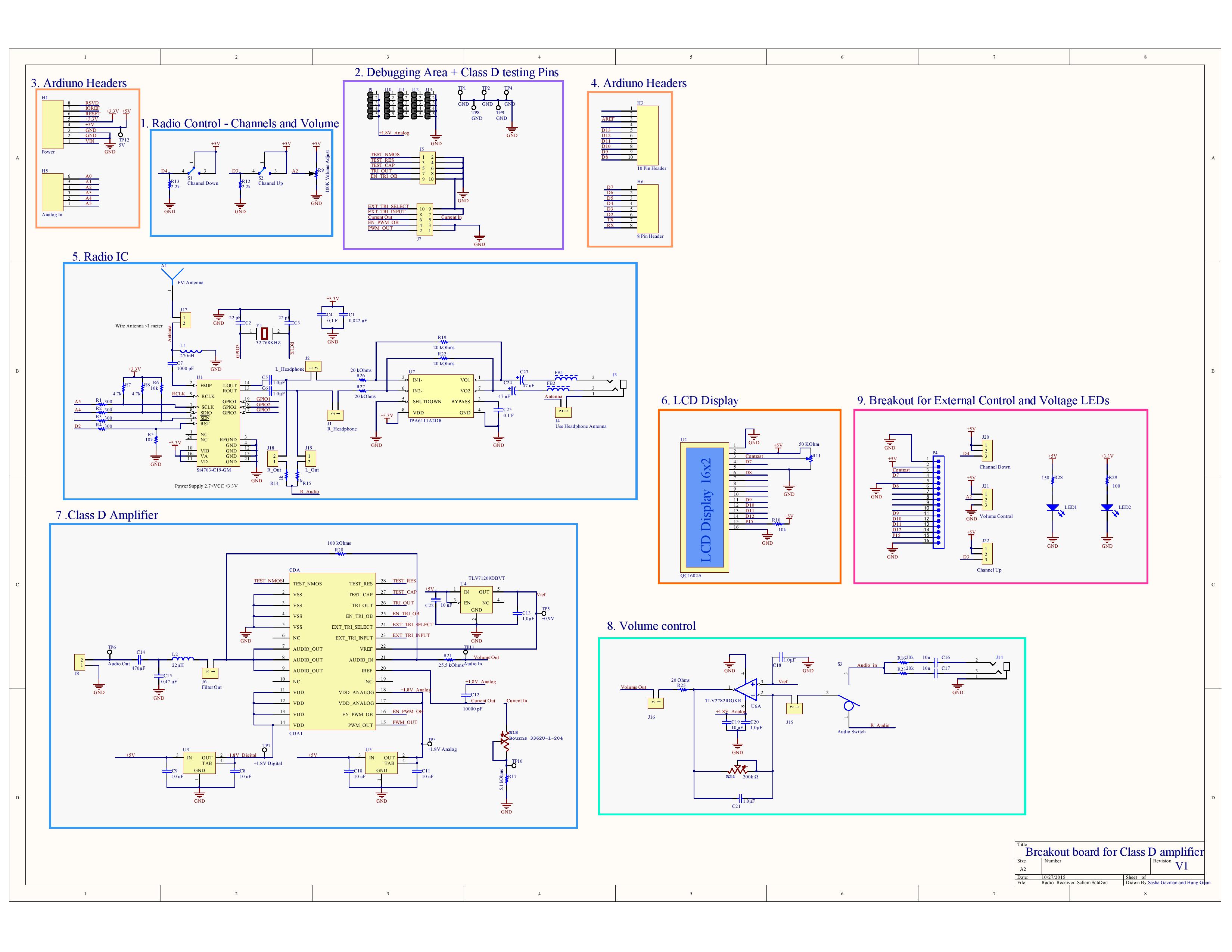
Fig. 1: PCB Schematics
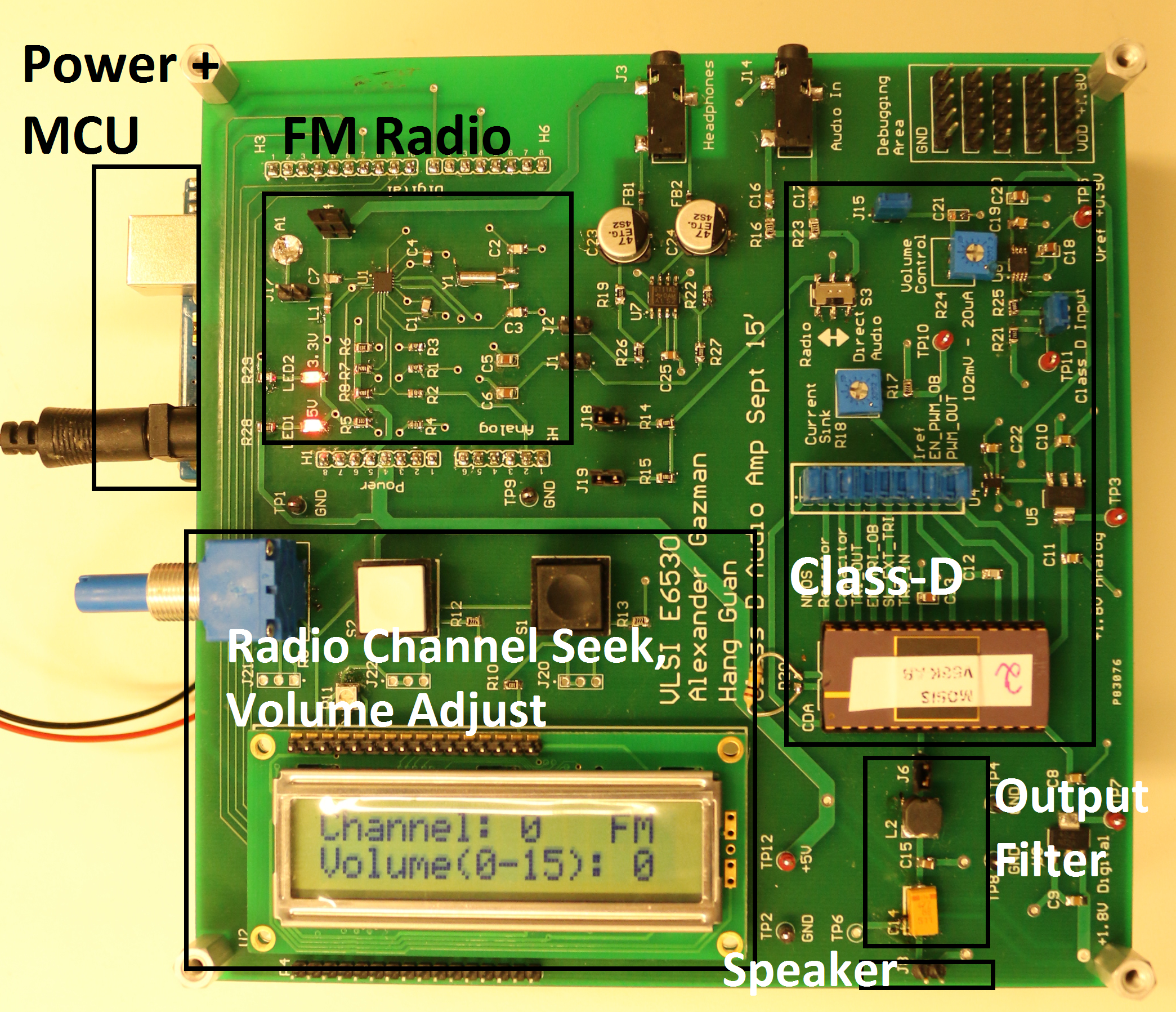
The physical layout of the board is shown in figure 2. The total area of the board is 6" x 6", with an additional Arduino board attached in the bottom layer. Modular ability was taken into consideration in the design - most of the blocks in the desgin are independent of each other, therefore, the board can be assembled partially while still getting its full functionality. The latest release of the project can be found and downloaded from the CircuitMaker community under the Columbia _VLSI_AH653 tag.