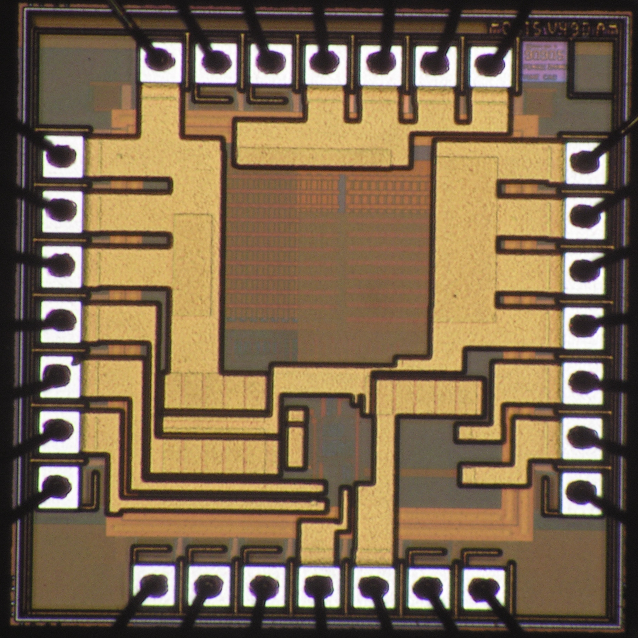
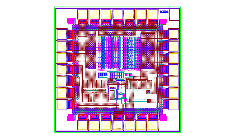
IC Layout
The picture below is the IC layout of the entire design chip. Four pins were used as VDD, four for ground and four for PWM output. The blocks were distributed along the die to minimize the trace resistance to the pins, and arranged to follow the signal flow through the system.
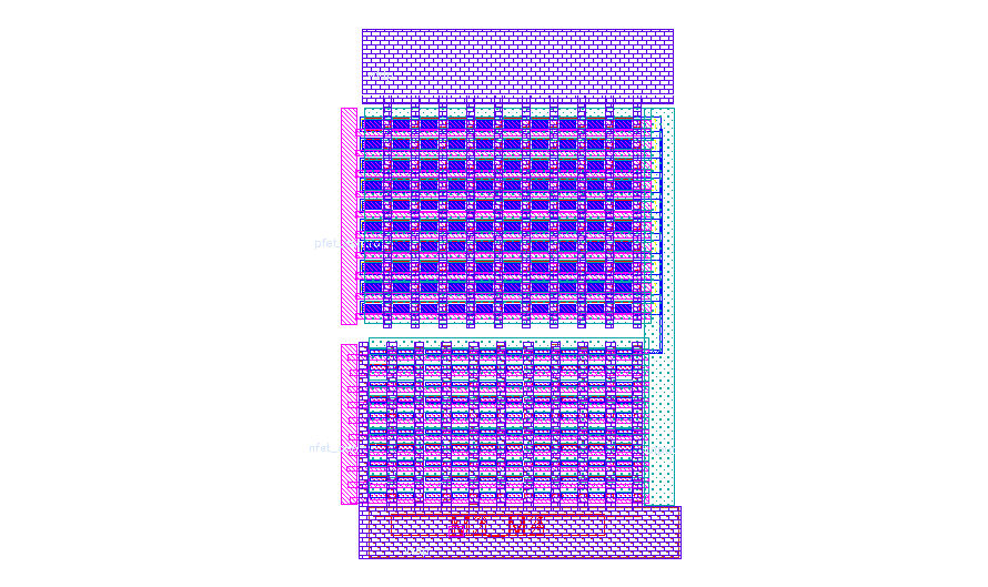
The picture below is the layout of the output stage. Starting from the top, the layout consists of the VDD bus, the PMOS, the output bus, the NMOS and the VSS bus. Both NMOS and PMOS are transistors arrays to provide enough driving ability and increase the efficiency.
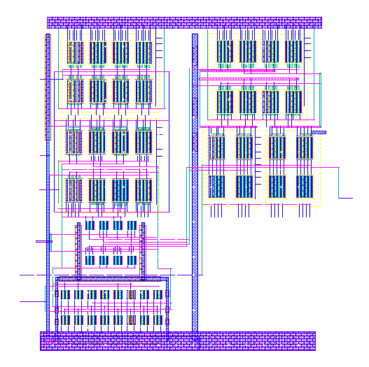
The picture below is the layout of the OTA. Input transistor pairs are arranged to share same centroid.