Design Verification and Testing
Simulation and Design Verification
All the blocks are simulated and verified individually at block level and at the top level. Simulations include AC, DC and transient analysis depending upon the functionality of individual blocks. Initially all the blocks are verified at schematic level and then RC parasitic extracted simulations are run. Each of the blocks are tested and verified with the typical and worst results using the parasitic RC extracted netlist is shown in table.1.
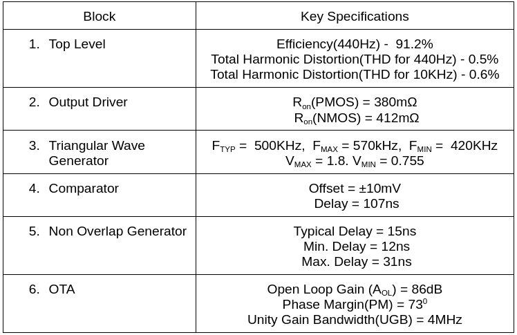
Table 1
Typical waveforms for the input and output for the whole chip top level are shown in fig. 1. As we can see from the waveforms, the input and output are out of phase because of the inverting nature of the circuit. But this really does not impact the audio performance of the circuit.
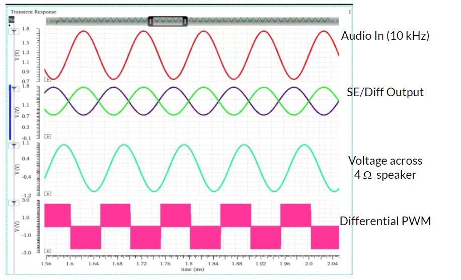
Fig.1. Simulation of Circuit At Top Level
Post Silicon Testing
The chip is mounted on a PCB using a socket. The PCB is designed using KiCAD. Fig.2 shows the schematic of the PCB. Programmability for each of the currents and various test points are being used to check and debug every signal. Additional triangular wave generator is also used in-case the inbuilt triangular wave is not working. The VDD is supplied by using buck converters and potentiometer is used for volume control.
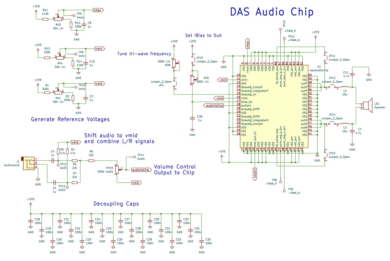
Fig 2. Schematic of the PCB
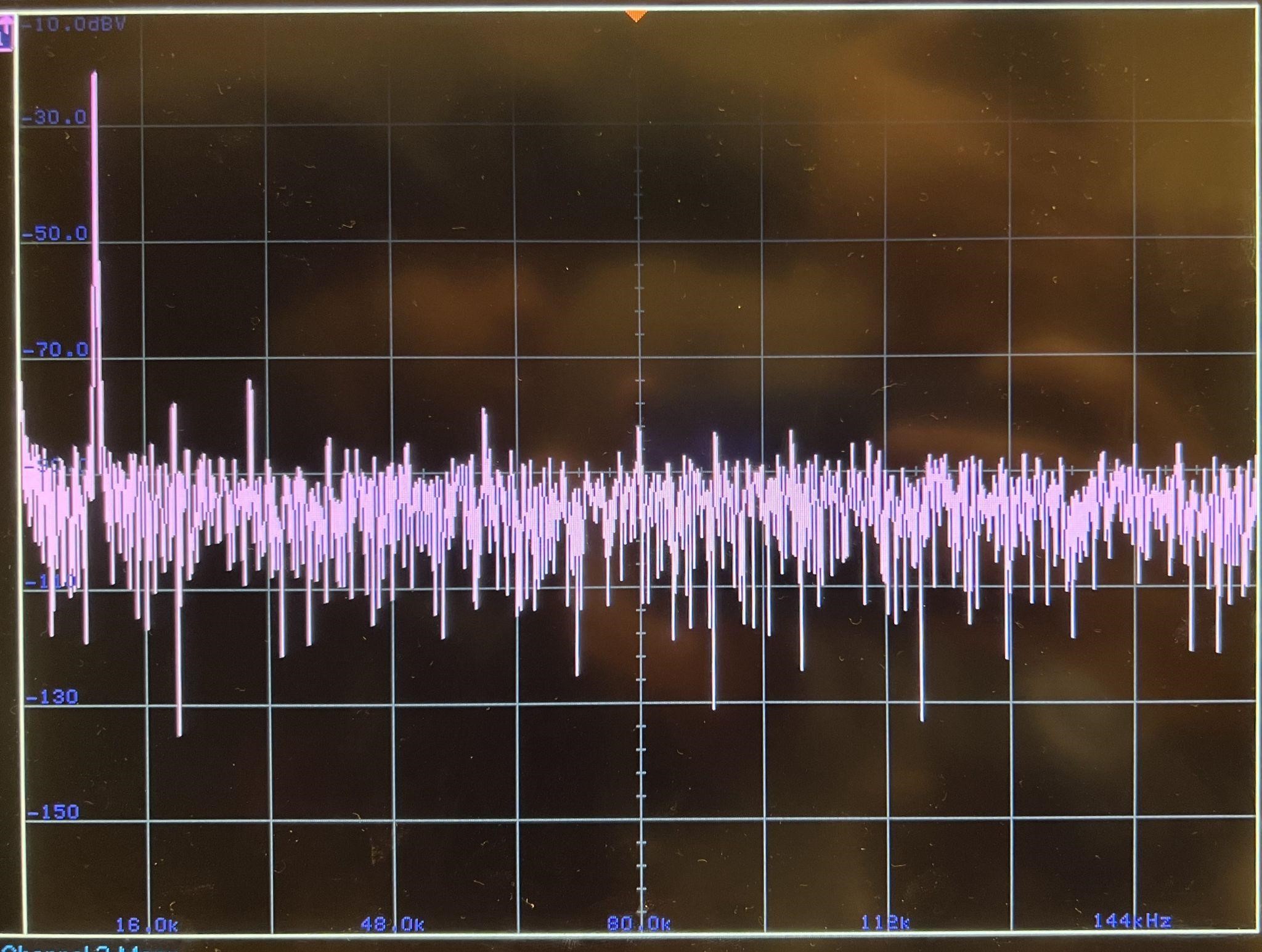
Testing is carried out for checking the robustness of the system. The triangular wave is carefully adjusted such that the frequency is close to 500KHz. Then the audio signal is applied. Typically one would start with a famous tone of 440 Hz and then the voltage waveform is observed. Fig. 4. shows the waveform viewed on the scope. We can see that the waveform looks very clean. Similar waveforms are also observable at higher frequencies as well. Various tests can be performed to assess the performance of the system. These include the THD(Total Harmonic Distortion) and efficiency test. THD is a quantitative measure of the presence of the other harmonics rather than the applied input. Since our case is a differential, the even harmonics would be hardly present and the THD is dominated by the odd harmonics.
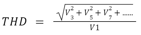
Here V1, V3, V5 are RMS values of the voltages at fundamental, third harmonic and fifth harmonic respectively. Modern oscilloscopes have the features of measuring the THD directly. This feature is used here to measure the value of the THD. Fig 3 below shows the testing setup.
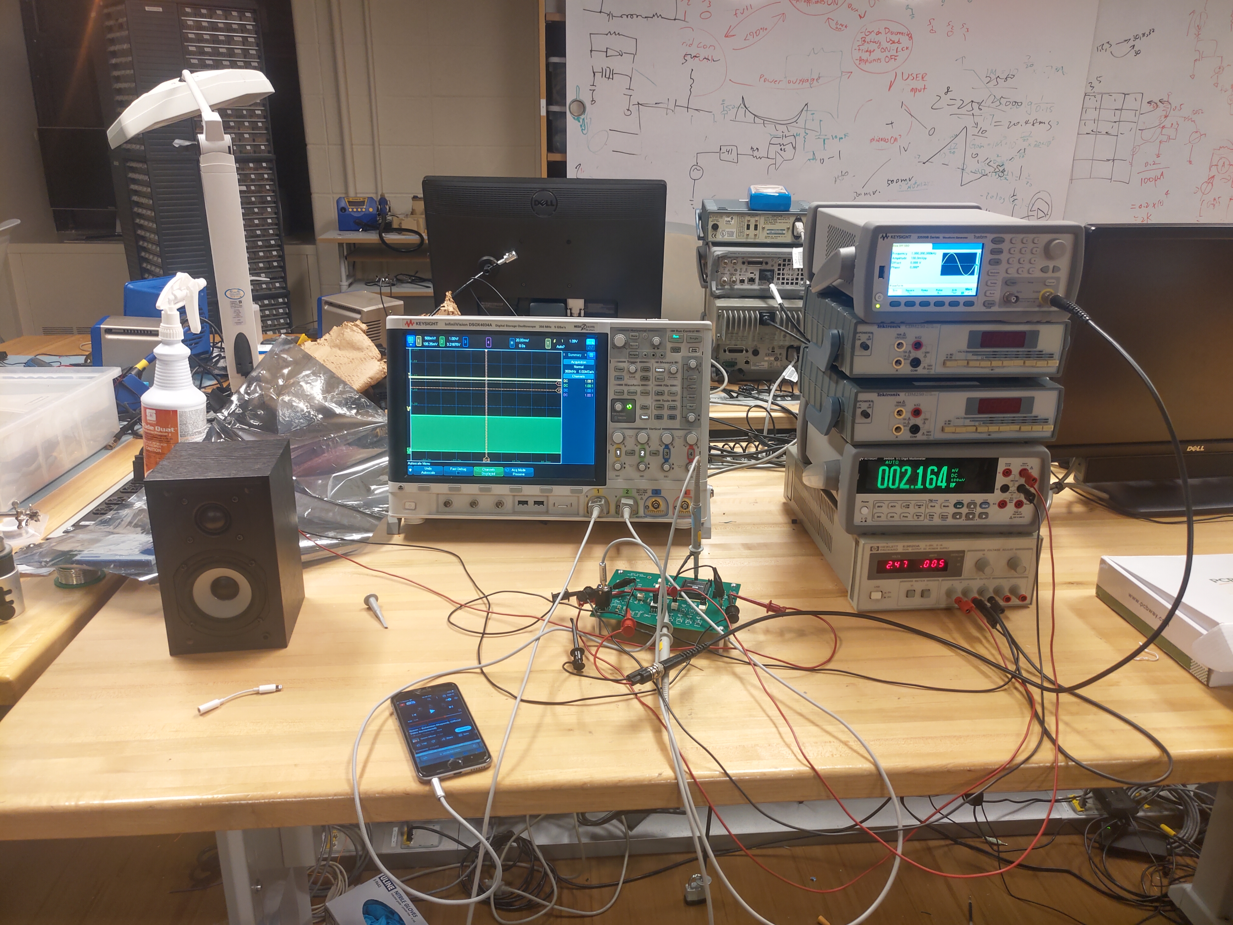
Fig.3. Test Setup

Fig.4. Output Waveforms
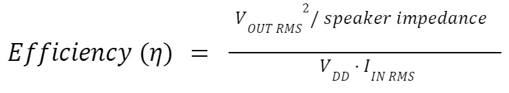
Another important measure would be efficiency. Efficiency is a quantitative measure of how much power is being burnt inside the chip without producing the useful work. Here the useful work would be power given to the speaker.
Both the analyses were across various frequencies and across various load impedances. Fig. 5, Fig. 6 shows the THD plots for various frequencies for 4 Ohm and 8 Ohm loads respectively. It can be seen that the THD is less than 3%. From this we can see that the audio clarity would be very clear which is evident in the video.
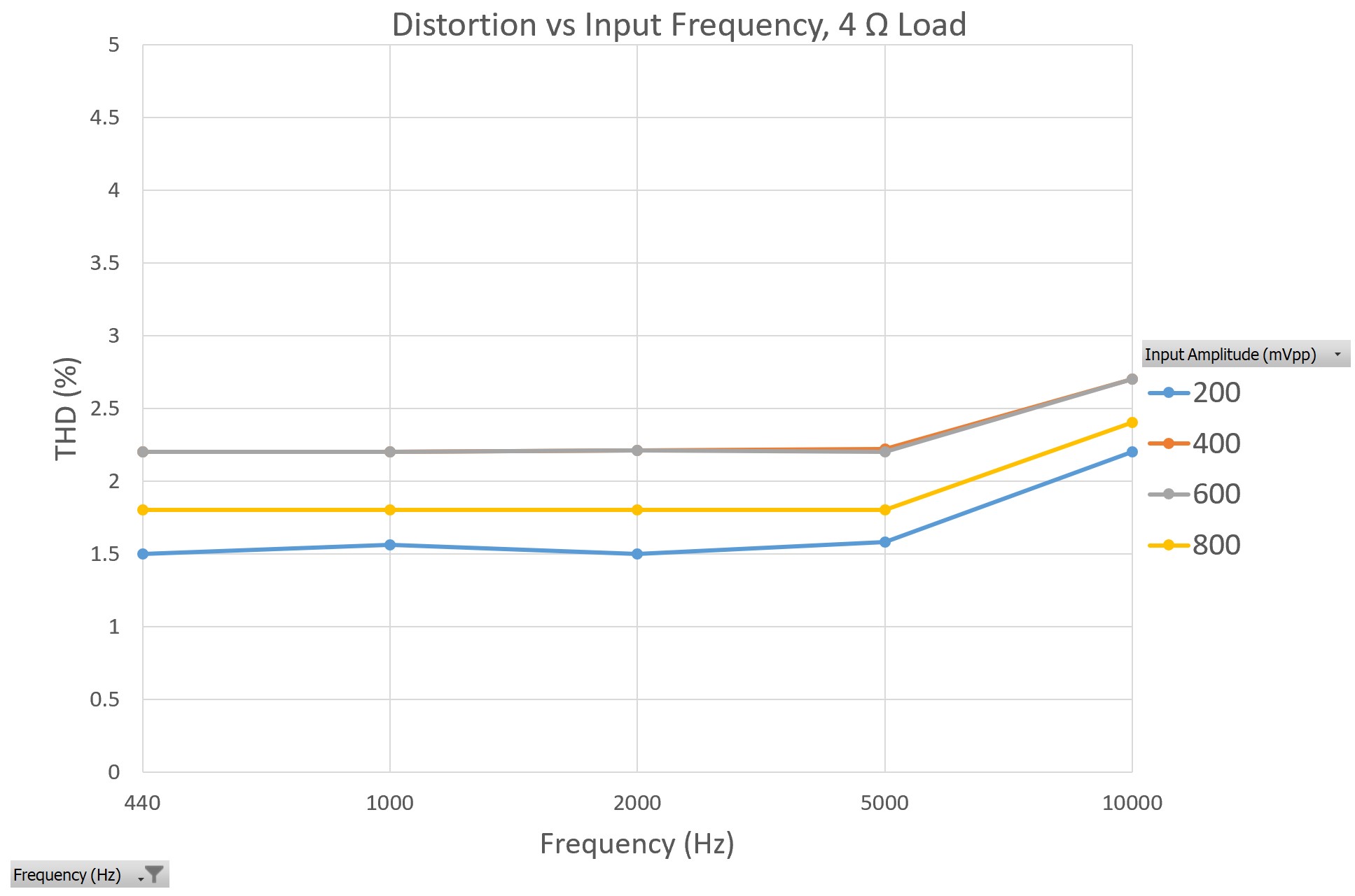
Fig. 5. THD vs frequency for 4 Ohm load and for various input amplitudes
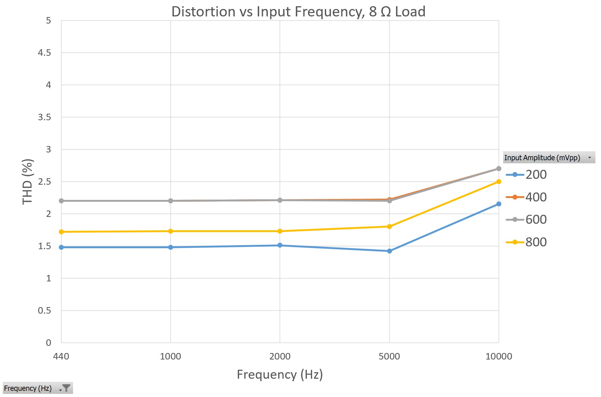
Fig. 6. THD vs frequency for 8 Ohm load and for various input amplitudes
Fig. 7 and Fig. 8 show the efficiency plots for various frequencies for 4 Ohm and 8 Ohm loads respectively. The efficiency is more than 90% at lower frequencies. But the efficiency drops as we go to higher frequencies. This is because of the more losses during the switching.
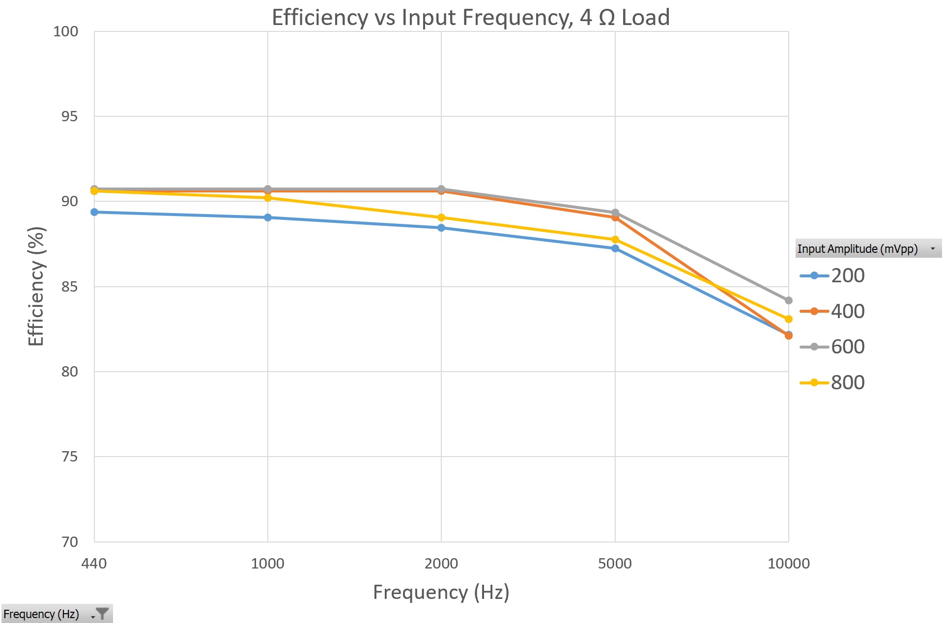
Fig. 7. Efficiency vs frequency for 4 Ohm load and for various input amplitudes
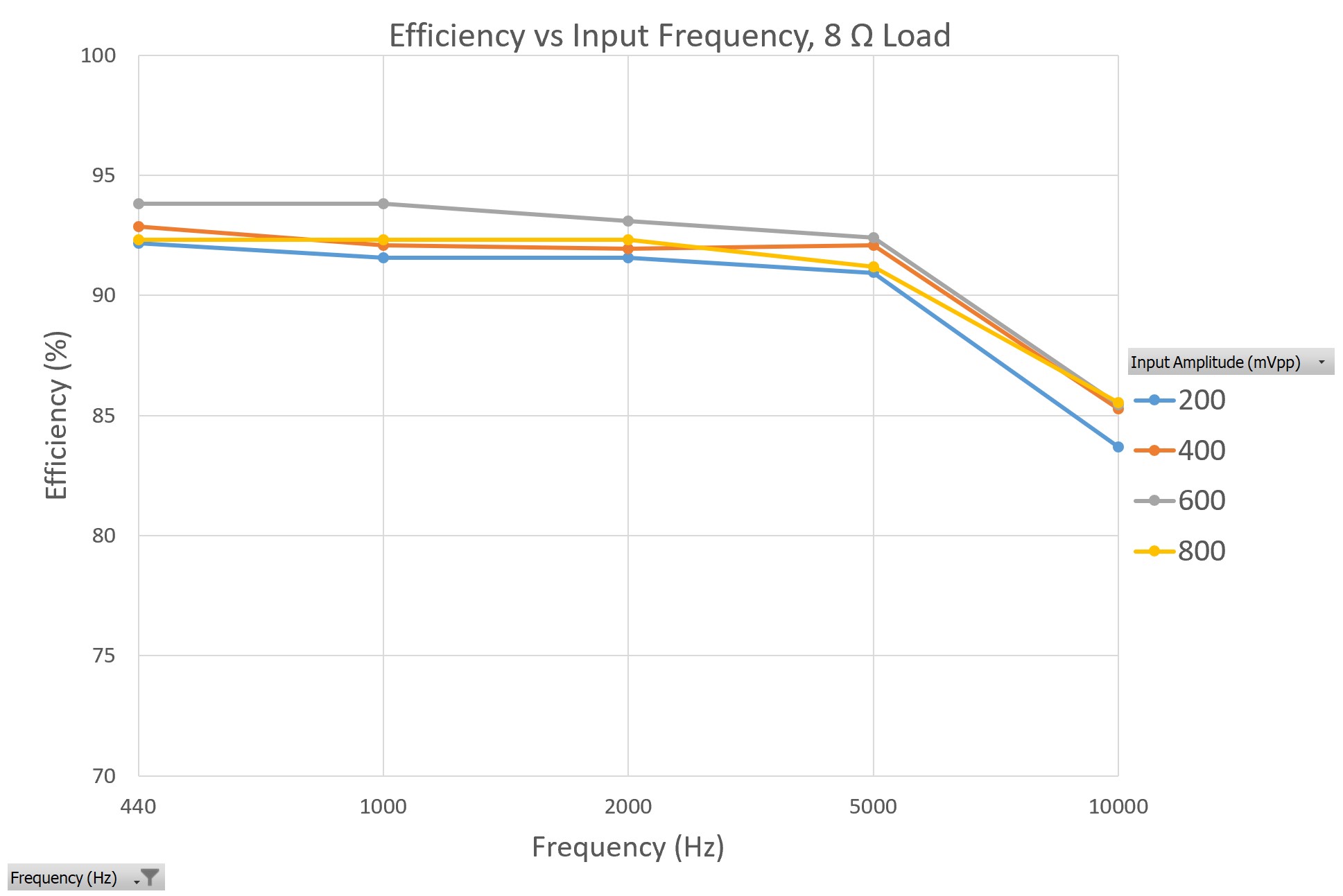
Fig. 8. Efficiency vs frequency for 8 Ohm load and for various input amplitudes
The spectrum of the differential output signal is also captured using the oscilloscope and then FFT is used to convert the time domain signal to frequency domain signal. Fig. 9 and Fig. 10 show the FFT plots for the input signals of 5KHz and 10KHz respectively.
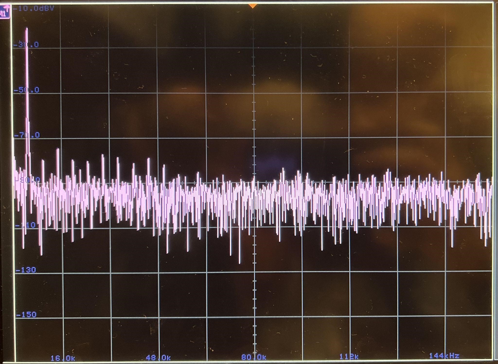
Fig. 9. FFT of Output Signal at 5KHz input