
System Overview
System Architecture
.jpg)
Fig 1. System Architecture
Fig.1 shows the system architecture of the audio amplifier chip. As told previously, the operation of the amplifier is in class-D mode. Here the final switches act as a power boosting stage. The signal path flows from left to right. The audio signal is converted into 2 differential signals using a single ended to differential converter. Then each of the signals are integrated and compared with a triangular wave. This leads to square pulses as outputs which are known as PWM signals. Then, the signals are fed to non overlap generators which lead to pulses whose rising or the falling edges are delayed. Those pulses are fed to buffers which drive the big switches. In the above block diagram, the non overlap generators, buffer drivers and the big switches are shown as a single block called as output driver. The top level schematic in Fig. 1 (in Block Description) shows an extensive description of each block. The non-overlap generators are required because if the clock pulses driving the big switches are having a common rising and falling edge, the low-side and high-side switches would turn on simultaneously and it would lead to a short from VDD to ground. This in turn leads to loss in efficiency and also leads to a lot of power being burnt. The specification and design of individual blocks are described further.
System Level Design

Fig.2. Simplified Block Diagram For System Design
Fig.2. shows the simplified block diagram of the single ended audio amplifier system. For the fully differential structure, the same diagram is applicable and is repeated twice and Vout being connected differentially. If we model the loop assuming an ideal integrator with a UGB of ωUGB,int and the PWM and output driver as a block that introduces a delay τ and a gain of GPWM, the loop gain can be written as
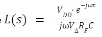
where
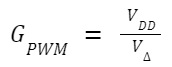
,
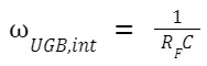
Here VΔ is the amplitude of the triangular wave.
Thus leading the loop gain to be:
The loop gain goes to 1 at ω:
The phase at this frequency is given by:
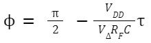
If we set VDD = 2.25V, VΔ = 0.8V and RF = 200 kΩ, and C=13.2 pF we can tolerate 40 𝝻s of delay for a phase margin of 60o. The result is valid until the UGB of the opamp is pretty large. Hence we have chosen at least 1MHz of BW and 50dB of gain.