Block Description
Chip Top Level
The whole chip is laid out in an area of 1mm x 1mm. However the available area for placing the circuitry was 900um * 900um. All the circuits are operated at 2.5V and hence mostly 2.5V devices are used. Fig. 1 shows the schematic of the top level.
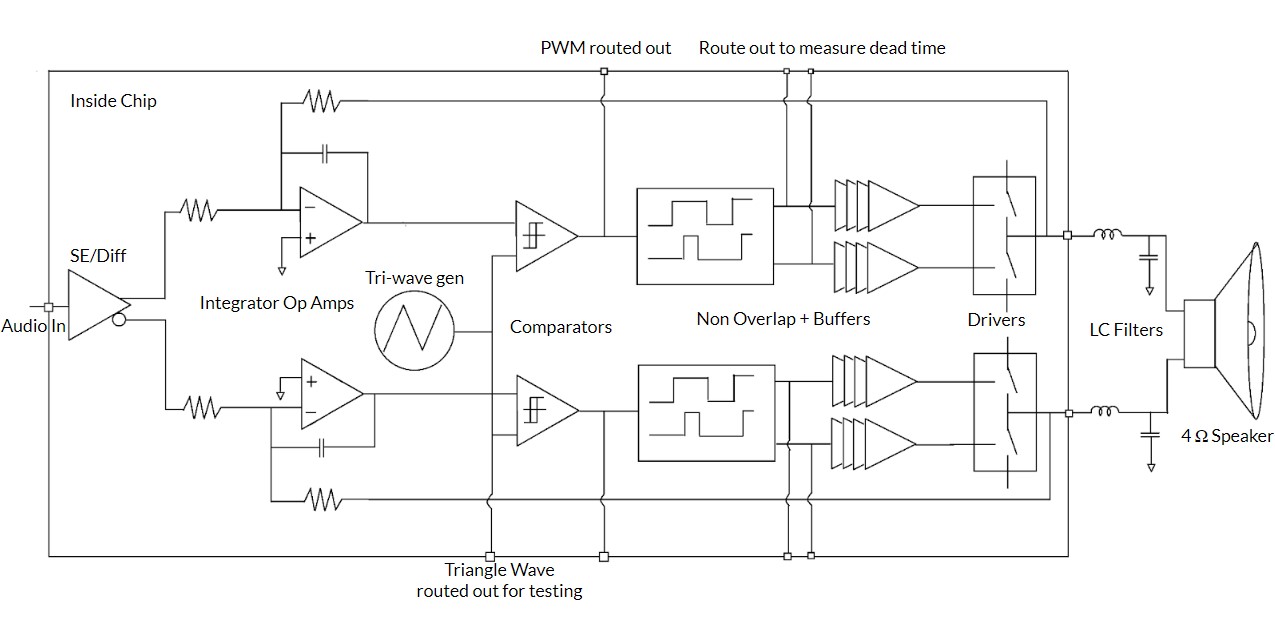
Fig.1. Top Level Schematic
The outermost rectangle shows the chip boundary. The LC filters, speaker, reference voltages for Op Amps and the triangular wave generators are placed outside the chip.
The layout is placed in such a way that there is always an axis of symmetry. The whole chip is placed in such a way that it is symmetric with respect to x-axis. Blocks like comparator, triangular wave generator, op amps are individually laid out such that they are symmetric with respect to y-axis. Fig.2 shows a simple floor plan of the entire chip.
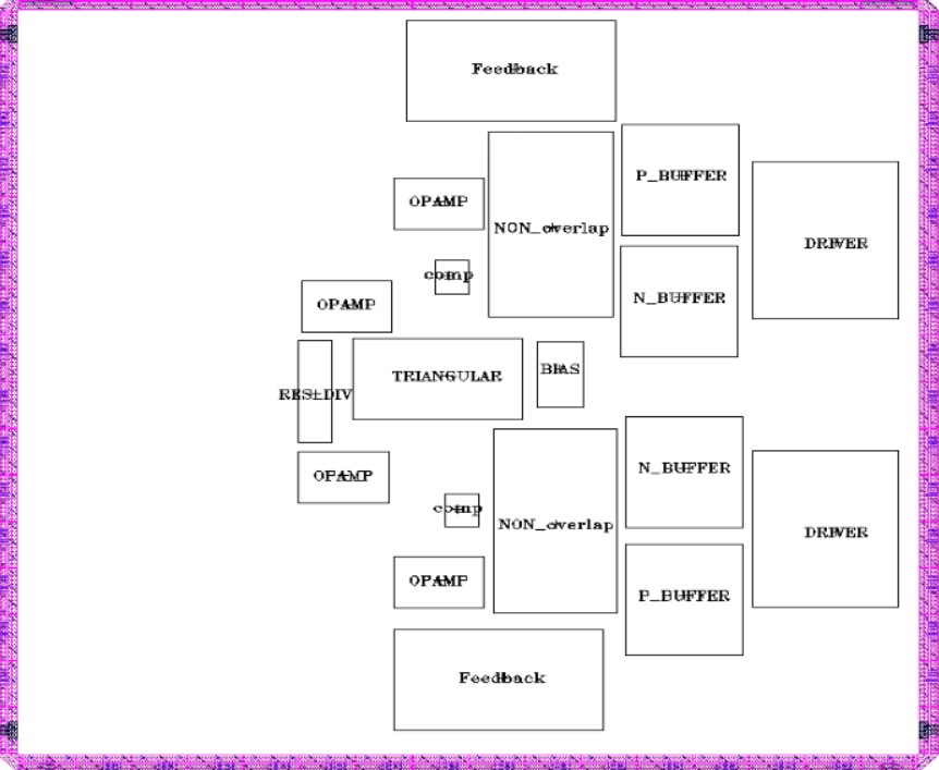
Fig.2. Top Level Floor Plan
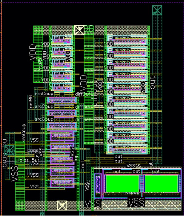
Fig.3 shows the top level layout including the bond pads. The blocks are spaced out and are placed with large metal traces in between so that they can deliver power more efficiently. The empty spaces are placed with decoupling caps so that they prevent ground bouncing due to large switching current through the bond-wire inductances. The VDD and ground are routed using the M8-M9 layers. The VDD and ground nets are routed in the form of mesh throughout the chip such that they form low impedance paths for the power and ground nets. Fig.4 shows the die photo.
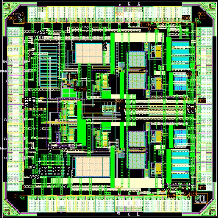
Fig.3 Chip Top layout
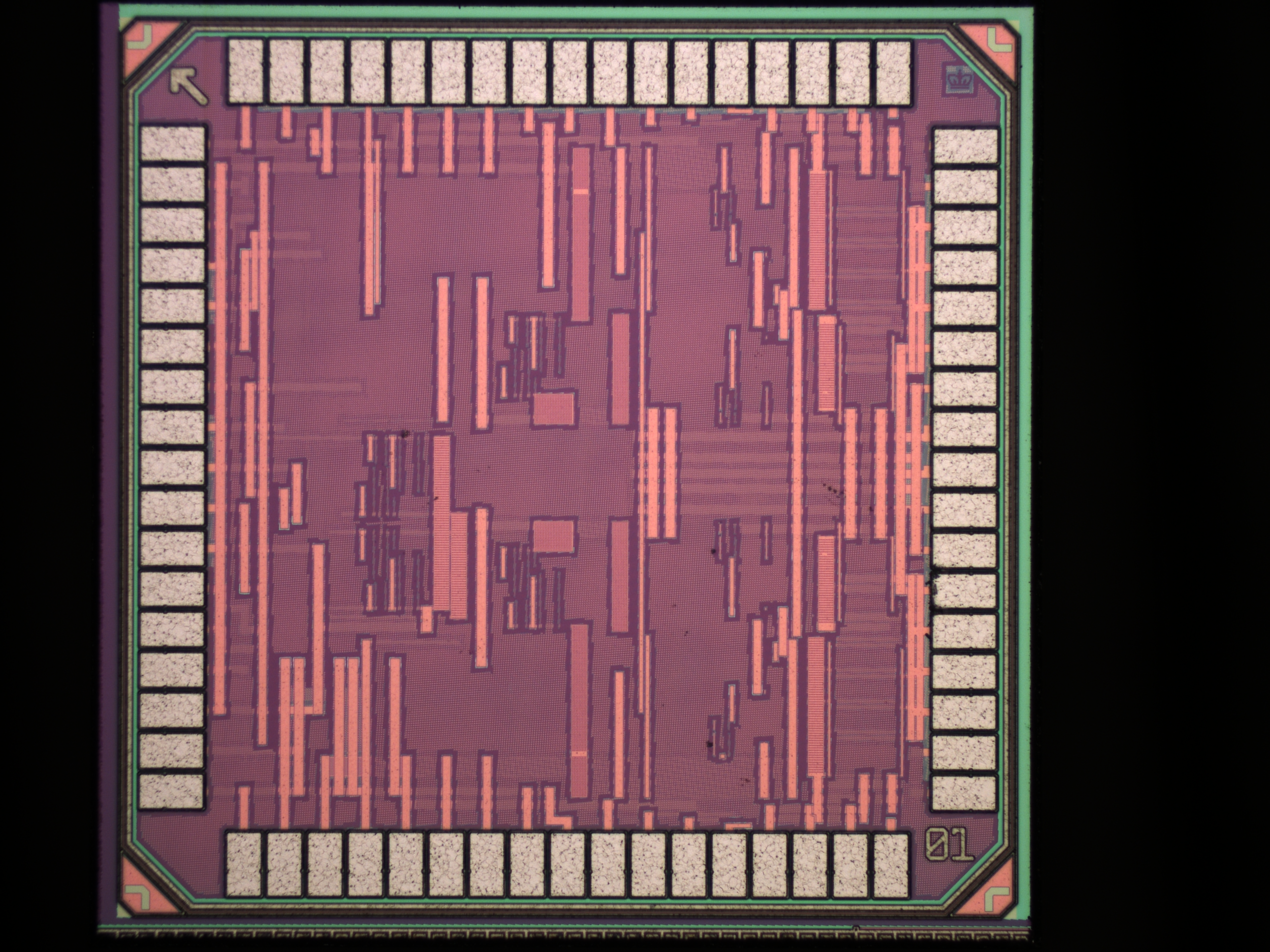
Fig.4 Die Photo
Output Driver (Big Switch)
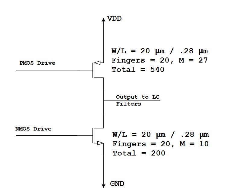
Fig.5.Output Driver
Fig.5. shows the size of the output driver switches. The switches are chosen such that it has to drive the 4 Ohm speakers with the required output voltage. Here 2.5V devices are used as our power supply is 2.5V. Minimum length transistors are used as there will be minimum switching losses. The maximum Ron for the PMOS is 380mΩ and for NMOS it is 412mΩ. Fig.6. shows the layout of the output driver stages. The top one is the PMOS and bottom one is NMOS. Proper well ties are used with bigger contacts to avoid latch up.
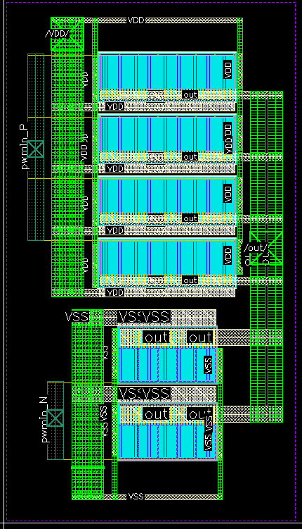
Fig.6. Output driver stage layout
Triangular Wave Generator
This is based on the architecture of the relaxation oscillator as shown in Fig.7. This circuit is used to generate the triangular waveform which in turn is used in the translation of input signal to a pulse width modulated wave. The period of oscillation is determined by the slew rate in charging and discharging the capacitor. It is given by I/C. Here the VMAX and VMIN are generated external to the chip using the resistive divider network. The layout is made as shown in Fig 8. The triangular wave generator typically generates 500KHz output frequency. The maximum frequency achieved was 579KHz and minimum frequency was 418KHz across PVT.
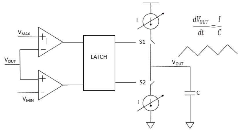
Fig.7. Triangular Wave Generator
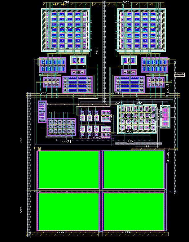
Fig. 8. Layout of the triangular wave generator
Comparator
This is based on the architecture of the relaxation oscillator as shown in Fig.9. This circuit is used to generate the triangular waveform which in turn is used in the translation of input signal to a pulse width modulated wave. The period of oscillation is determined by the slew rate in charging and discharging the capacitor. It is given by I/C. Here the VMAX and VMIN are generated external to the chip using the resistive divider network. The layout is made as shown in Fig 10. The triangular wave generator typically generates 500KHz output frequency. The maximum frequency achieved was 579KHz and minimum frequency was 418KHz across PVT.
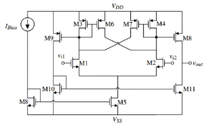
Fig.9. Schematic of Comparator
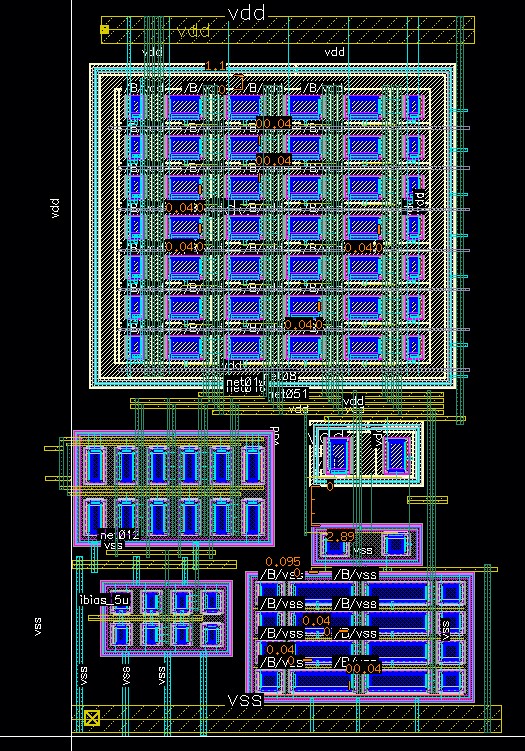
Fig.10. Layout of the Comparator
Non Overlap Generator
Non overlap clock generators are used to create clock pulses whose edges will never overlap at the same time. They always have some amount of delay between them. The design of the non-overlap generator is relatively straightforward. The only thing we need to keep in mind is the delay chosen has to be optimum. If the delay is less, then the edges will overlap and if the delay is more, then distortion in the sound will be more. Here an optimum delay of 15ns is chosen which varies with PVT and parasitic extraction from 12ns to 31ns. Fig.11 shows the schematic of the non-overlap generator. The delay is generated using the capacitor - inverter chain in the feedback of the latch so that they get triggered at different times. Fig. 12 shows the layout of the non overlap generator. The layout is big because the capacitors are implemented using the MOM capacitors and occupy a large area.
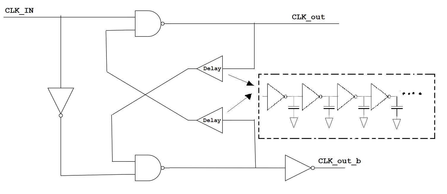
Fig.11.Schematic of the Non-Overlap Generator
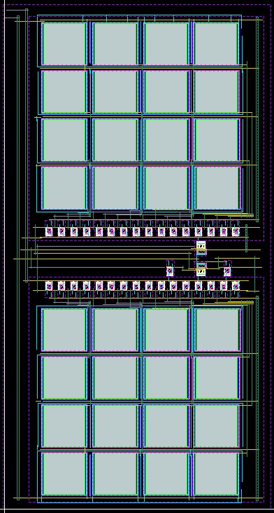
Fig.12. Layout of the Non-Overlap Generator
OTA
The Operational amplifier is used as an integrator in the loop. The Opamp is also used to convert the signal from single ended to differential signals. Here the opamp used is a simple standard architecture with a miller compensation and a nulling resistance. Fig. 13 shows the schematic of the opamp used in the chip. Fig.14 shows the layout of the opamp. The opamp typically has a gain of 86dB, UGB of 4MHz and a phase margin of around 70o.
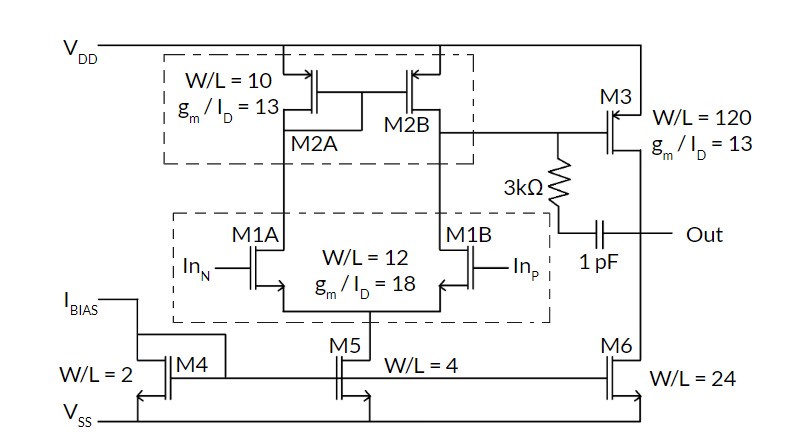
Fig.13. Schematic of the Opamp