
Testing
A computer program was written to communicate with the PCB as well as all the testing equipments (voltage source, current source, signal generator, etc.), so that the configuration and testing of the chip could be done automatically.
Rail-to-Rail-Input-Output Amplifier
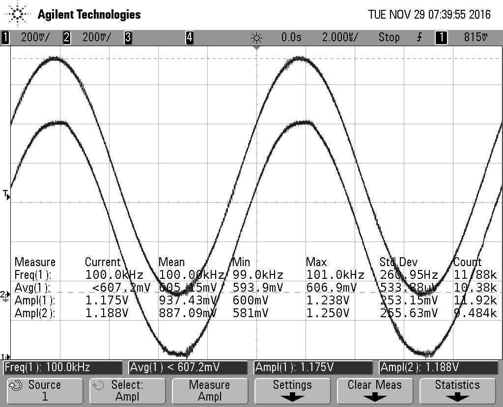
The rail-to-rail-input-output amplifier is configured as a unit gain buffer (shown in Fig. 10). The waveform is shown (in Fig. 11) when the input is a rail-to-rail (1.2V peak-to-peak) sine wave, and the output can reach almost the rails except for some tiny deformation.

When the input voltage is decreased by 30mV in amplitude, there is no longer any visible distortion (as shown in Fig. 12).

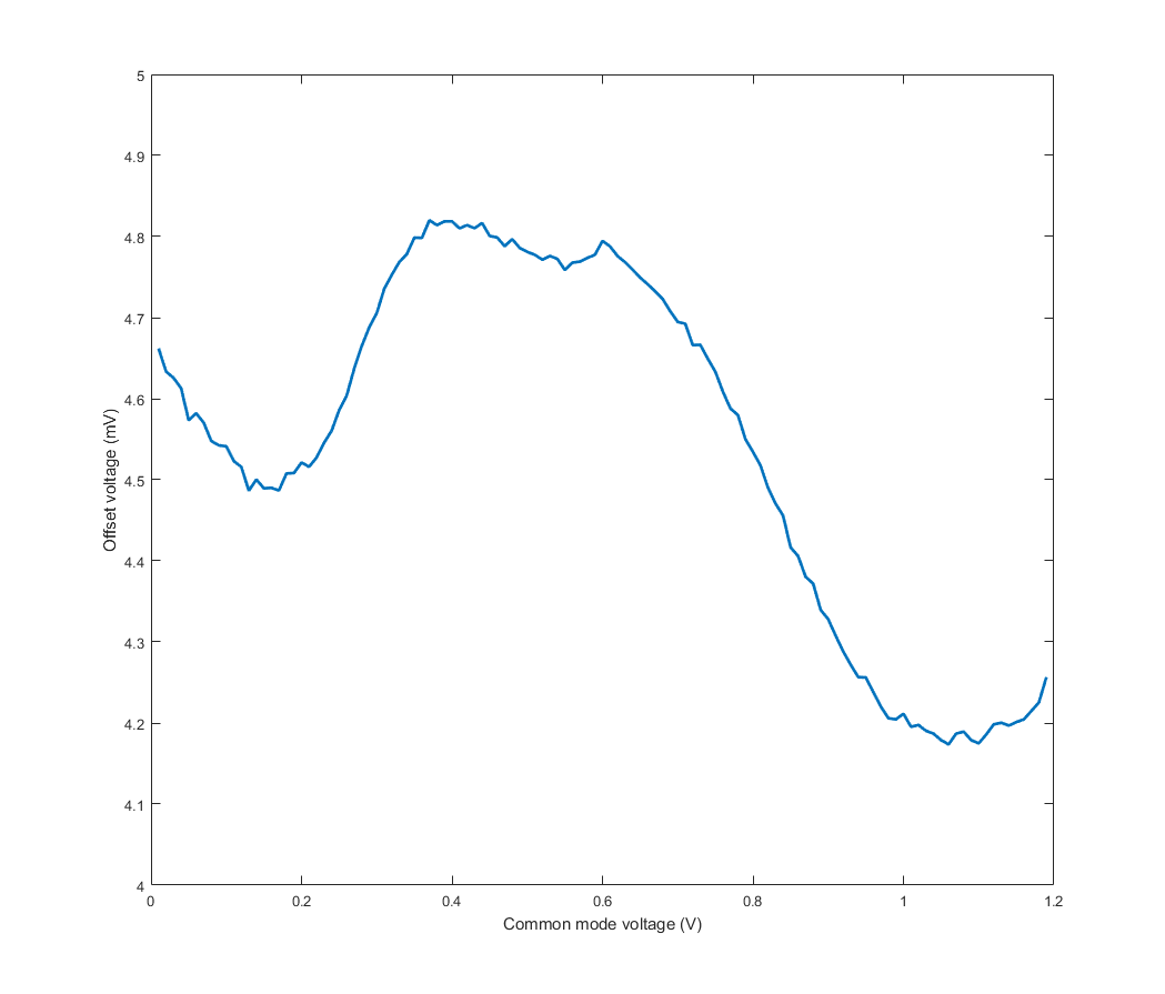
Another measurement was carried in order to measure the DC characteristics of this amplifier. The two input terminals were biased with an external high accuracy voltage source (Yokogawa GS200), and the output voltage is measured using a multimeter (Hwelett Packard 34401A). The extracted DC gain and offeset is shown in Fig. 13, Fig. 14 and Fig. 15.
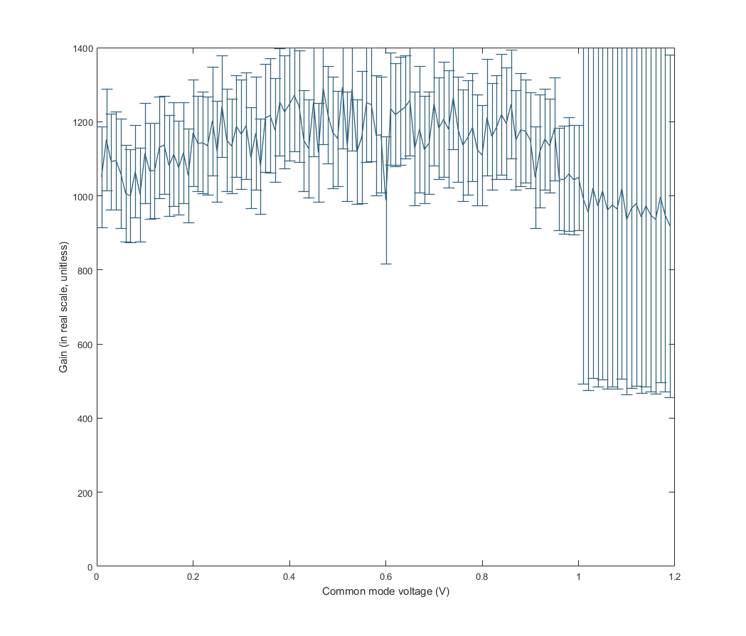
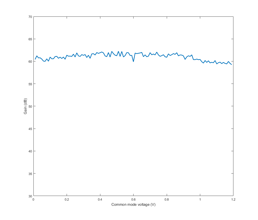
The measured gain with a common mode voltage higher than 1V has a un-compensated systematic error that will make the measured gain lower than the real value. This is because of a drop in the precision of the voltage source.
In general the rail-to-rail-input-output amplifier works as expected.
Current Integrator Based Transimpedance Amplifier
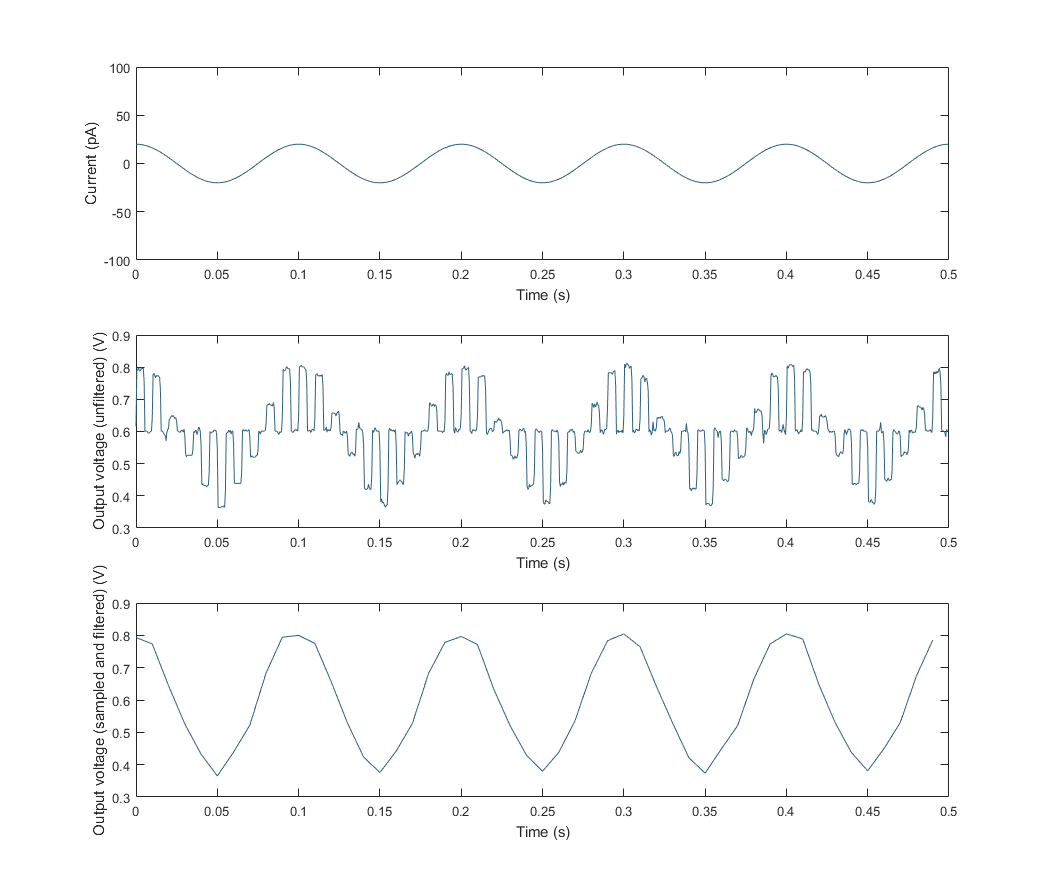
Fig. 16 shows the output waveform of the current integrator based transimpedance amplifier, when a 40pA 10 Hz peak-to-peak current sine wave was applied to the input. The current integrator samples the input current at 100Hz. The top plot shows the input signal, and the second plot shows the output read from the oscilloscope. The majority of the noise seen on this plot comes from that of the oscilloscope. The bottom figure presents the voltage during the hold time as a single value. From the measurement, the gain of the transimpedance amplifier with a clock of 100Hz is about 10GOhm, which is about 25% lower than what is predicted by theory.
Another measurement is done with square waves of 2Hz, and an amplitude of 500fA and 200fA respectively. The results are shown in Fig. 17 and Fig. 18 respectively.
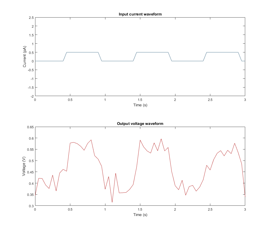
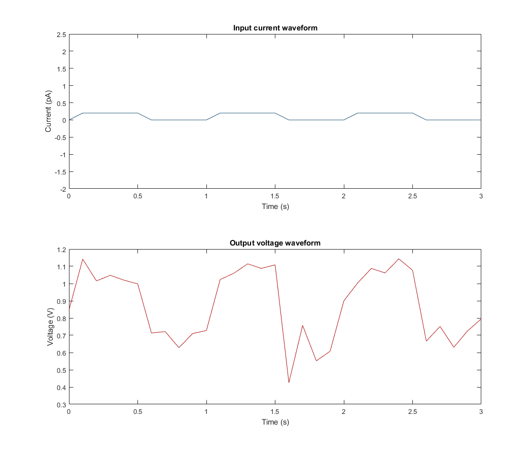
The current amplifier works worse than what was expected from simulation.