
IC Layout
OTA Layout
The layout of a single OTA is shown in Fig. 6.
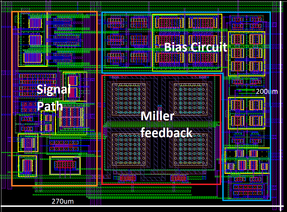
In this layout, the bias circuits are at the side of the layout, with only wires running current signals comming out to reduce potential noise coupling. Transistors, capacitors and resistors that needs to be matched carefully are all layed out in a common centroid mannar. The length of the path for the signal to run is minimized, and differential nets are put as close as possible to reduce possibilities of coupling differential mode noise. Pseudo power grid is designed to minimize power distribution resistance.
Capacitor Array Layout
The layout of the capacitor array is shown in Fig. 7.
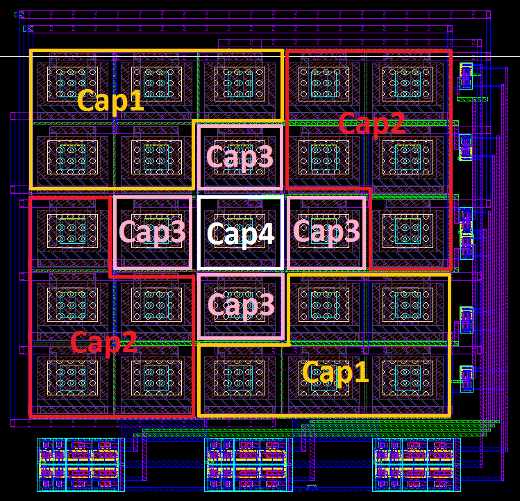
The capacitor array is connected in a way that creates 4 different capacitors with a capacitance ratio of 10:10:4:1, forming an 5 by 5 array of capacitor C0. All connections are made in a way that the 4 capacitor share a common centroid. One of the capacitor with a value of 10C0 is connected as the sample capacitor CS in the second stage and as the tracking capacitor CT of the third stage. The other three capacitors are connected in the corresponding feedback loop with switches. By changing the amount of capacitance showing in the feedback, this capacitor array creates a variable post integrator gain (n in the second stage, and m in the third stage). The possible gains are 10, 2.5, 2 and 1.