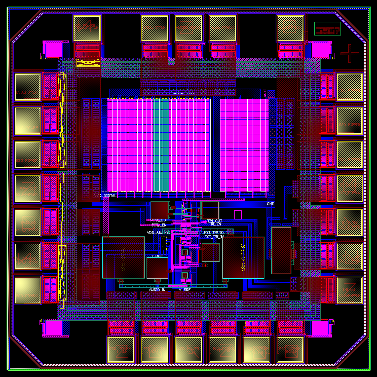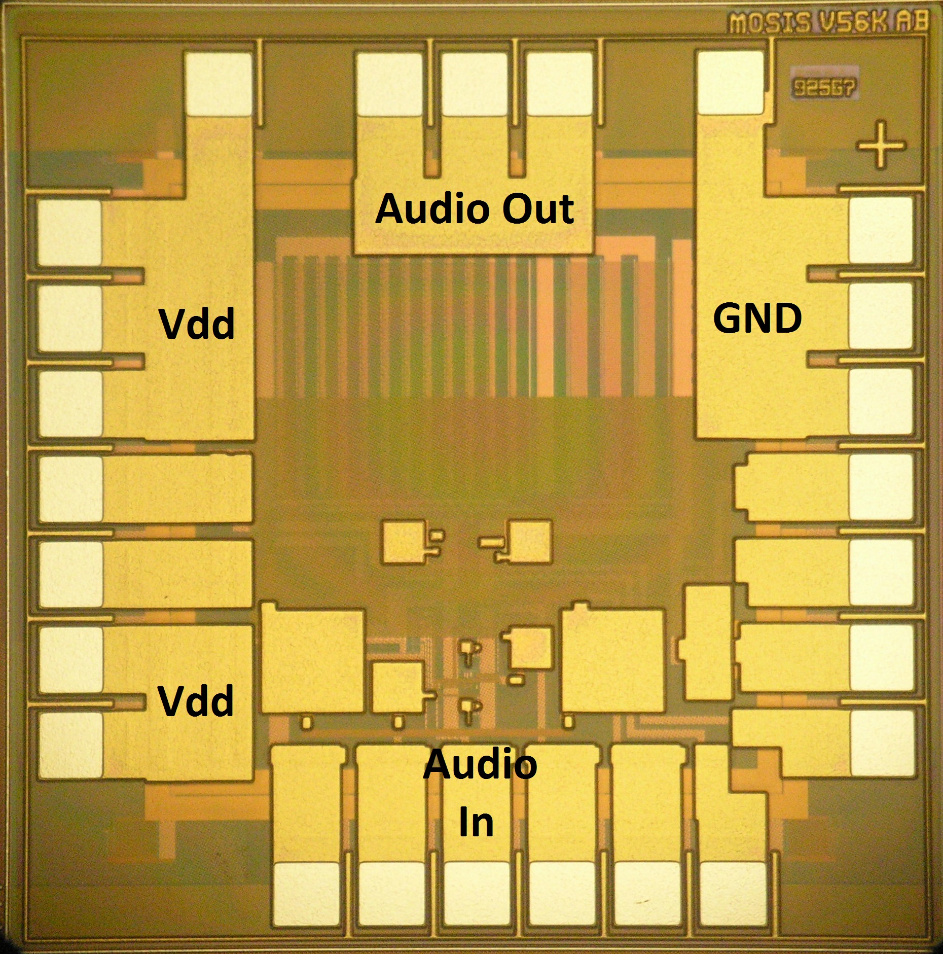
Layout
This amplifier was layout using IBM 180-nm RF CMOS process. It was fabricated in MOSIS foundry and packaged using MOSIS DIP28 package. The layout size is 1500 x 1500 microns. Top-level layout is seen in Fig. 1. The signal enters from the bottom side of the layout and exits from the top. A "+" marker at the top-right is used to indicate the orientation with respect to the package.