
System Overview
Class D audio amplifiers have gained much popularity during the recent years due to their high efficiency and low power consumption. In the mobile space, Class-D amplifiers are used for headset speaker since they can be fully integrated into CMOS process.
Traditional linear amplifier amplifies the input sinusoidal signal using active devices in linear (saturation) region. In Class-D amplifier, the signal to be amplified at the output devices is a series of pulses. The input signal is first converted to a series of pulses by pulse width modulation. The PWM wave is then amplified with active devices in either on or off state. The pulse width contains the lower frequency audio information. At the output the amplified output pulses is passed through a low pass filter to convert back into analog signal.
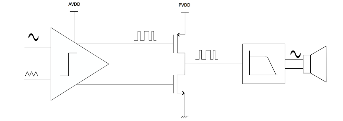
The Class-D amplifier can generally be represented by the Figure 1.
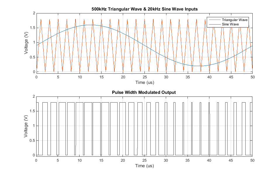
The comparator performs the modulation with the sinusoidal input. Figure 2 demonstrates the transformation. The comparator designates a high signal when the sine wave is higher than the triangular wave input, and vice-versa. The result is a pulse train with a duty cycle that corresponds to the instantaneous value of the input sine wave. This is the pulse width modulated (PWM) signal that will be amplified.
The frequency spectrum of the PWM signal with a 1kHz signal shows the input signal spectral content is preserved, while the switching frequency carries the audition tone. Nyquist theorem dictate that the sampling request must be at least twice of the input spectrum, but for a low distortion design switching frequency is usually 5 to 10 times.
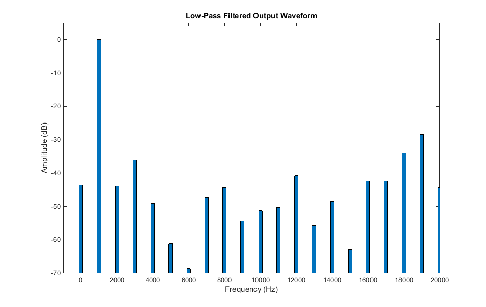
After a low-pass filter on the PWM waveform, one can expect the spectrum in Figure 4. There are no major harmonics, and the highest one would be at least 30dB below the fundamental tone.
In the general Class-D amplifier as in Figure 1, the DVDD for the output stage is typically higher than VDD of comparator, thus the PWM signal is shifted up to provide high output voltage swing and gain. This is not the case in CU6350 since a single VDD is used.
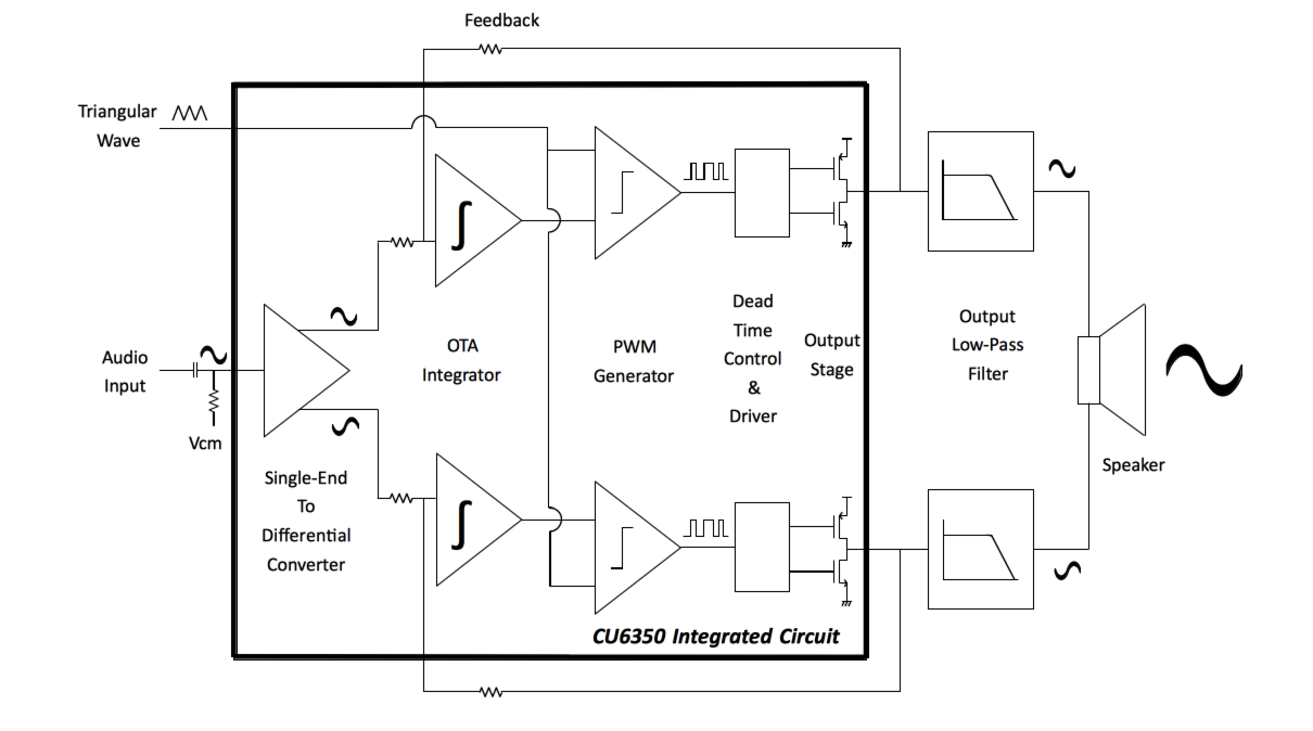
The general Class-D amplifier in Figure 1 does not have any mechanism to reject noise on the power supply, especially 60Hz hums that will pass thru the output low pass filter. The implementation of CU6350 creates a negative feedback loop that includes the output devices. Since any error within the loops is attenuated by the loop gain, a high loop gain will ensure the power supply noise is rejected. To achieve this high loop gain, an integrator is used. The integrator cut-off frequency is set to not include the switching frequency, so it is not attenuated by the loop gain, thus the output remains a PWM waveform.
To drive significant current into 8Ω speaker load, large out put devices are needed to ensure high efficiency. Due to the large input capacitance of these devices, preceding drivers will ensure quick transition. If the PMOS and NMOS are being turned on at the same time, a short circuit path will exist between VDD and Ground, and that will greatly reduce efficiency and possible damage the device. A Dead time will provide two non-overlapping waveforms for the NMOS and PMOS inputs, such that crowbar current is eliminated.
To combat low output power with 1.8V supply, a differential BTL output is used. Although the amount of on-chip hardware is doubled, the output power sees a four-fold increase. Differential output also eliminates the need of DC block capacitor when a 50% duty cycle PWM is present at the output. In addition, all even order harmonics will be cancelled when differential output is summed at the speaker output, driving the total harmonic distortion figure even lower.
The output LC filter provides a 2nd order low pass function. This will recover audio signal by averaging the PWM wave and attenuate the switching frequency. The output filter only needs to preserve the 20Hz-20kHz, and higher attenuation of the switching frequency will reduce distortion. However at cutoff frequency exactly at 20kHz will introduce unwanted phase shift. After careful considerations, the switching frequency is set at 500kHz, the integrator cut off is at 80kHz and the output filter is a butter-worth type cuts off at 28kHz.