Block Description
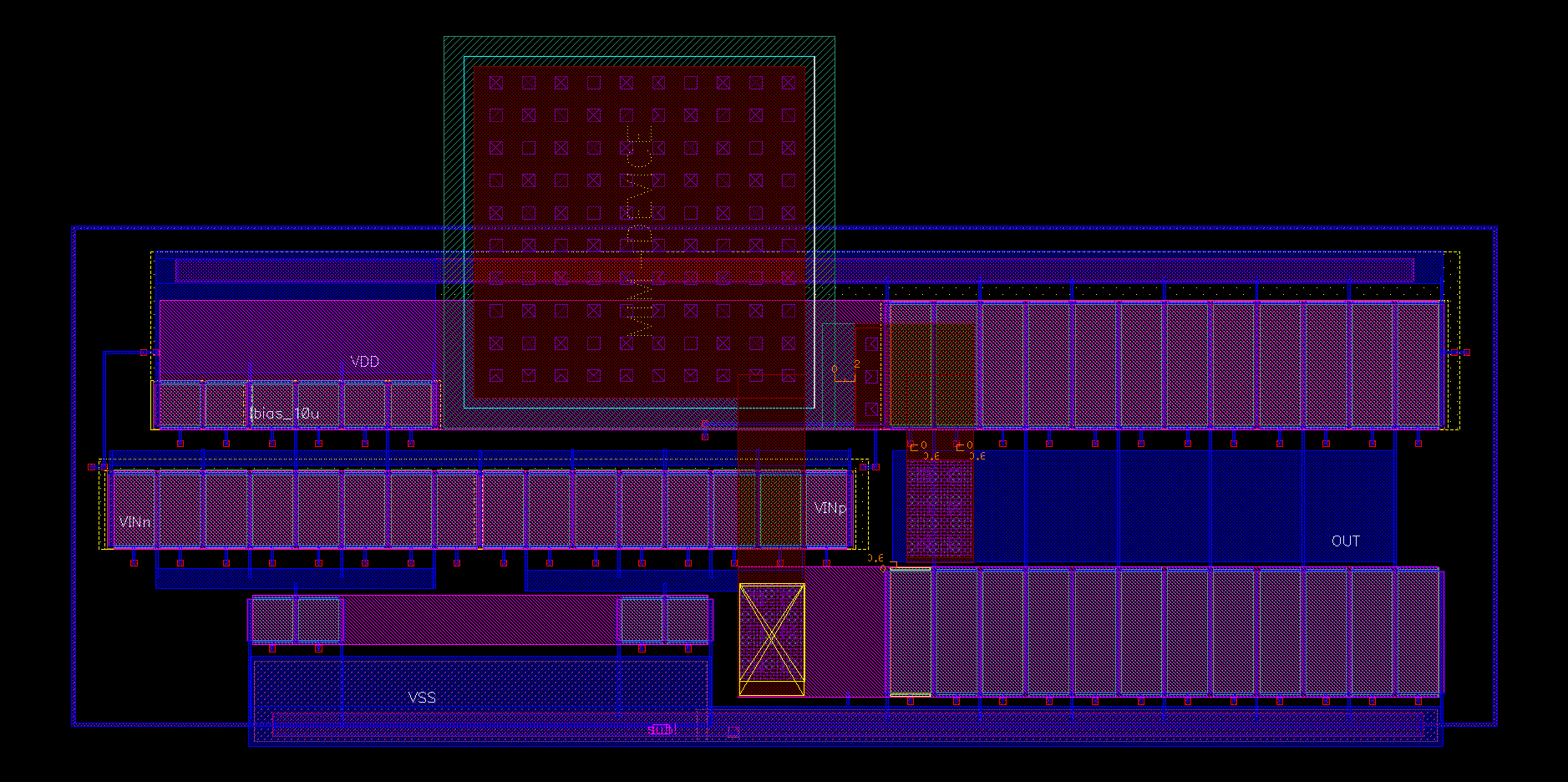
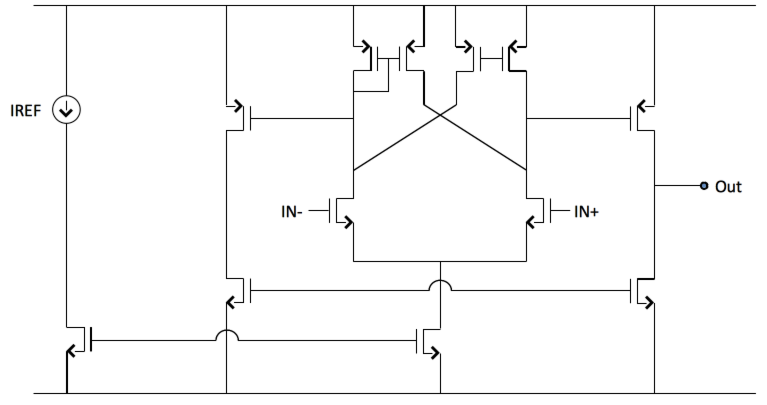
OTA
OTAs are required for the single-end-to-differential convertor and the integrator, so it has to be significantly high gain and stable across all operating frequencies. To simplify the design process, a single miller-compensated two stage OTA is designed and repeatedly used.
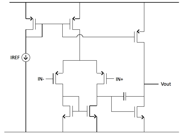
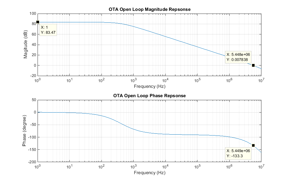
Simulation after layout extraction shows the OTA having a DC gain of 83.5dB, gain-bandwidth-product of 5.45MHz and phase margin of 46.7degree.
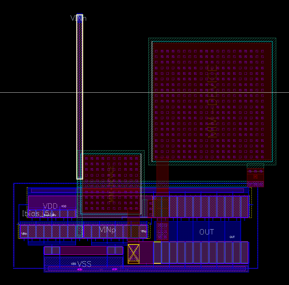
Single-ended to differential converter
Two OTA in negative feedback are cascaded to form the single-end-to-differential converter. The first is connected as unity buffer and the second is an inverter amplifier with gain of 1. This ensures that the input signal is subjected to the high impedance of the PMOS and phase relationship remains the same for both paths. At this point in the layout, all stages are designed for symmetrical placement.

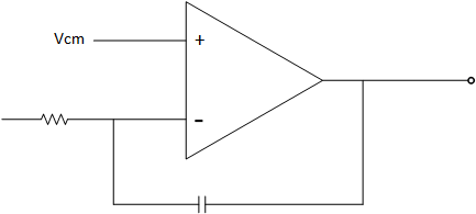
Integrator
The integrator is formed as an OTA with capacitive feedback. The transfer function is, T(s)=(A(s))/(s(R_F C_F)) , where A(s) is the open-loop transfer function of the OTA. The MIM capacitor consumes considerable amount of area and has a 20% variance in fabrication, so a trade-off is made to locate the large resistor (250k) externally to accurately control the response.
PWM modulator
The PWM modulator generates the waveform by comparing the input signal with a triangular wave as described above. The speed of the comparator is critical because the triangular wave input frequency is 500kHz, which has a period of 2us. This means the comparator must settle to its value within 1% of the period, or 20ns to reduce distortion. The design uses a small signal differential stage loaded by a PMOS latch, and further buffered by a common source amplifier.
The latching PMOSs are critical for hysteresis control, so extra care was placed to ensure both latches have symmetrical length of M1 interconnect.
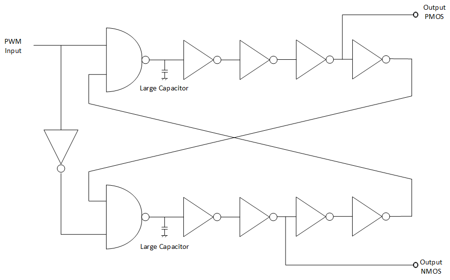
Dead time generator & driver
The dead time generator is a NAND-based non-overlapping clock circuit. This circuit produces the gate voltage such that during the dead time, neither the PMOS nor the NMOS at the output stage would be turned on, hence reducing the shoot through current. The dead time is determined by the delay within the inverter loop. The inverters are sized such that they receive a significant under drive from the previous stage. This allows the delay to realized, and also larger inverters will be used to drive the large output stage MOS.
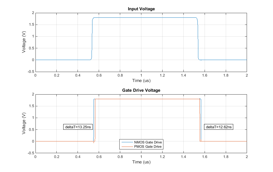
It was found that simply using inverter delay to get 1% dead time (10ns) is rather area inefficient. So an additional capacitive load is placed on the small NAND gate to reach the design dead time. After parasitic extraction, the simulated dead time ranges from 10.3ns to 15.7ns from slow to fast corners. The typical corner waveform is show in Figure 6, which dead time of 12.9ns.
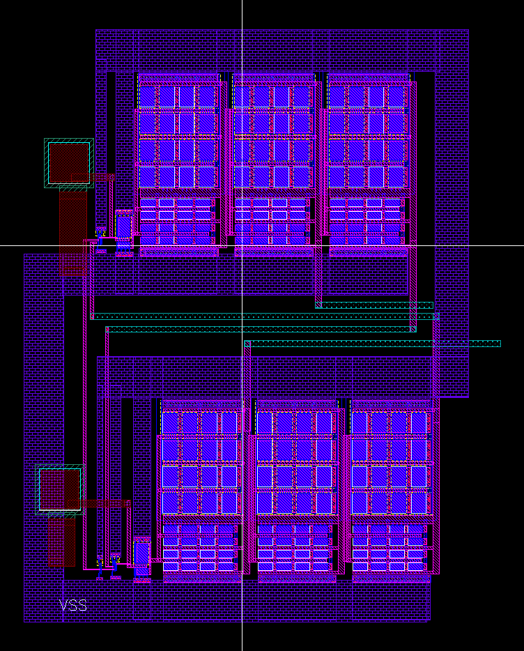
Output stage
The output stage consists of large multiples of fingered devices to reduce overall on-resistance of the MOS. Any loss in the output stage direct impacts the efficiency of the amplifier so the layout is also optimized for minimum interconnect resistance. The gates, drain and source of each MOS is connected by grids of metal interconnect, and a large number of vias and contacts are used. The loss during a high output at is measured as less than 2%.
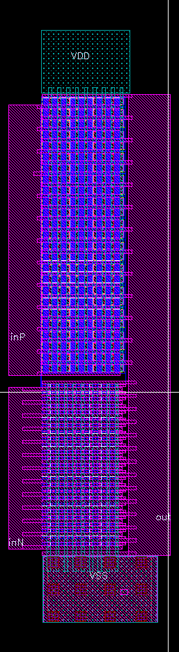
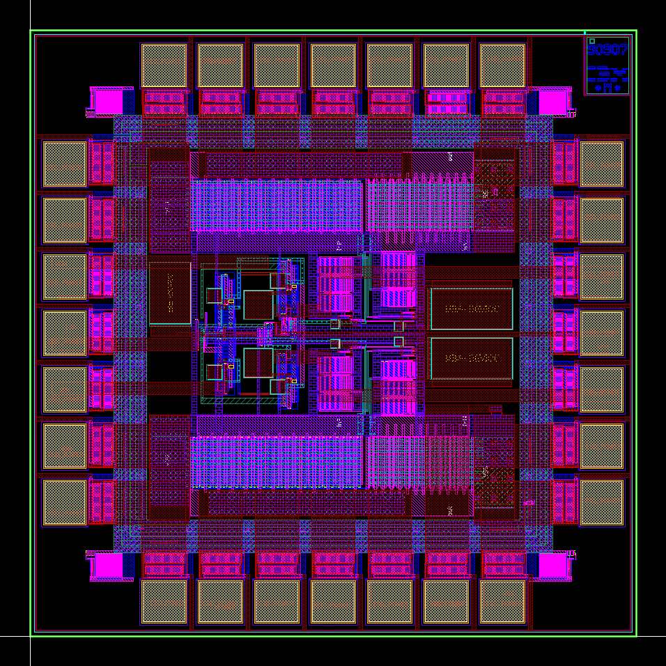
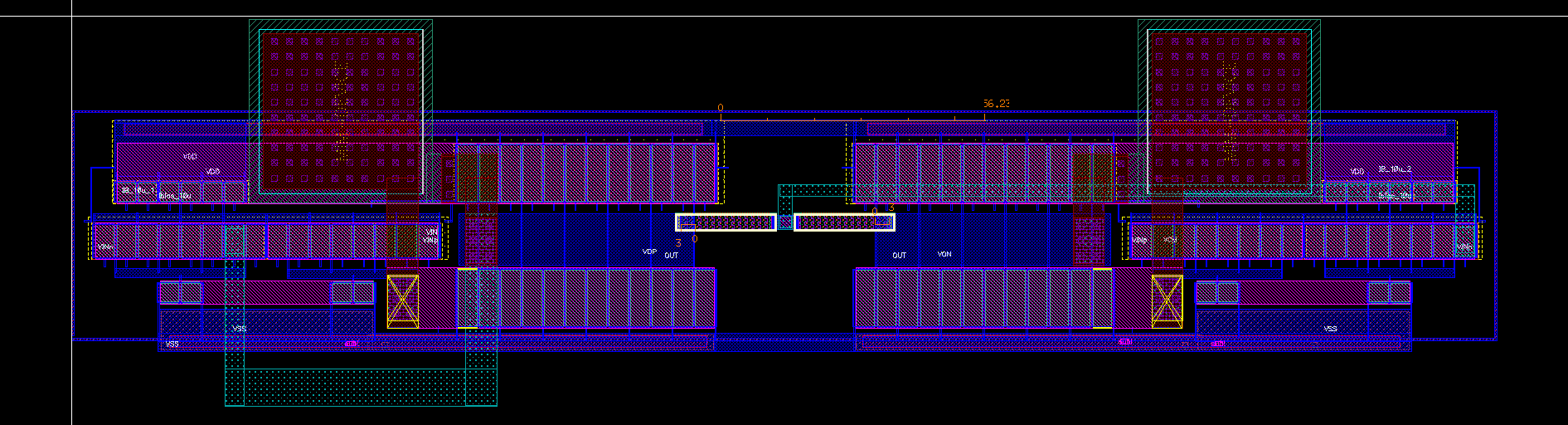
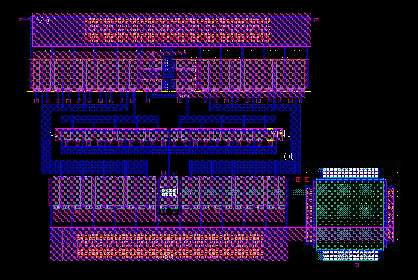
Overall layout
The overall layout of the chip consists mirrored blocks of the integrator, dead time generator and output stage, after the single-end-to-differential converter. It strives for symmetry because of the differential design. VDD and GND pins routes power from the corners of the chip, and outputs are on the top and bottom center pins. Signal inputs are routed via the left and right center pins to minimize power supply noise.